
D-Band PCB: Manufacturing Limits and Loss Budgets at 110–170 GHz
D-band PCB manufacturing: what 110–170 GHz does to loss budgets, thin-core tolerances, via stubs, solder mask and the boundary of coupon verification.
Home » D-Band PCB » D-Band PCB: Manufacturing Limits and Loss Budgets at 110–170 GHz
Table of Contents
D-band — 110 to 170 GHz — is where the PCB industry's usual vocabulary starts to fail. Wavelengths drop below 2 mm, copper skin depth drops below 0.2 µm, and the tolerances that were line items in a fabrication note at 10 GHz become first-order electrical terms. Recent D-band demonstration links have shown data rates in the tens of gigabits per second for point-to-point and data-centre interconnect, and every one of those links contains a PCB somewhere between the waveguide flange and the silicon.
The honest way to talk about a D-band board is with a loss budget and a tolerance stack, because those two documents decide whether the design survives contact with a fabrication line. This page computes both, from one stated model, and marks clearly what a PCB manufacturer can verify on a coupon and what belongs to the system integrator's fixture.
The model, stated once so it can be checked: 50 Ω microstrip on a 0.127 mm, εr 2.20 PTFE-class laminate, 1 oz copper, line width 0.395 mm, effective dielectric constant 1.87. Dielectric and conductor losses are computed separately; conductor loss uses the surface resistance of annealed copper with a roughness correction. At 140 GHz that line loses about 0.61 dB per 10 mm, and 70 % of it is in the copper, not the laminate. Everything in this guide follows from learning to read numbers like that one.
Material parameters for the laminate families — Dk, dissipation factor, thermal behaviour — are compared in the high frequency PCB materials section, with the PTFE family detail in PTFE materials and the low-loss hydrocarbon and ceramic-filled families in Rogers materials. This page is about what a fabrication line does to those numbers.
1. What Changes at 110–170 GHz: Geometry Becomes Electrical
Every frequency migration rescales the boundary between "a trace" and "a component". At 1 GHz that boundary is around a metre; at 28 GHz, around 5 mm; in D-band, the trace and the component are the same thing. The numbers in the table below are the whole reason D-band fabrication is a different discipline rather than the same discipline with a tighter tolerance.
| Frequency | λ0 (free space) | λg (εeff 1.87) | Phase | Copper skin depth |
|---|---|---|---|---|
| 110 GHz | 2.73 mm | 1.99 mm | 181°/mm | 0.199 µm |
| 140 GHz | 2.14 mm | 1.57 mm | 230°/mm | 0.177 µm |
| 170 GHz | 1.76 mm | 1.29 mm | 279°/mm | 0.160 µm |
Computed for 50 Ω microstrip on 0.127 mm, εr 2.20 PTFE-class laminate. Two consequences follow. First, geometry: a 0.10 mm segment of trace is 23 degrees at 140 GHz, so a feature that was invisible at 6 GHz is now a tuned element. Second, roughness: skin depth is 0.177 µm, and a standard electrode-deposited foil has a surface roughness of 3 µm — more than fifteen times the depth the current actually occupies. The conductor surface, not the laminate, is where most of the loss is decided.
The phase column is the one board designers feel first. A 0.10 mm difference in line length — the kind of dimensional tolerance that never appeared on a 6 GHz drawing — is 23 degrees of phase at 140 GHz. Matched-length routing, coupler spacing and resonator dimensions all now live at the same scale as the fabrication tolerance, which means the tolerance is no longer a manufacturing statistic; it is part of the circuit value.
The skin depth column decides where the loss budget goes, and it deserves a second look. At 6 GHz the current occupies the top 0.85 µm of the copper. At 140 GHz it occupies 0.177 µm — a layer thinner than a wavelength of visible light. Every profile feature of the copper surface, from foil tooth to plating nodule to the grain of the etch, is now large relative to the conduction depth, and the surface's roughness factor saturates near 2.0 for any ordinary foil. Sections 2 and 6 work through what that does to the budget and to the finish choice.
The third change is less visible but just as expensive: at these frequencies the dielectric constant is not a material property any more, it is a distribution. A ±0.02 lot tolerance on Dk, which nobody at 6 GHz would measure, is a ±0.7 GHz shift in a 140 GHz resonator — half a channel. Section 4 puts numbers on that.
2. Where the Loss Budget Goes at 140 GHz
Loss at D-band is not one number; it is two mechanisms with different physics and different owners. Dielectric loss scales linearly with frequency and with the loss tangent — it belongs to the material. Conductor loss scales with the square root of frequency through the surface resistance, multiplied by the roughness factor — and at D-band it belongs mostly to the geometry and the finish, not to the foil grade. The table splits them.
| Laminate class (εr / Df) | Dielectric | Conductor (ED foil) | Total per 10 mm | Per 100 mm |
|---|---|---|---|---|
| PTFE, low loss (2.20 / 0.0009) | 0.18 dB | 0.43 dB | 0.61 dB | 6.1 dB |
| Hydrocarbon (3.48 / 0.0037) | 0.99 dB | 0.58 dB | 1.58 dB | 15.8 dB |
| FR-4 (4.30 / 0.0200) | 6.07 dB | 0.67 dB | 6.75 dB | 67 dB |
50 Ω microstrip on 0.127 mm dielectric, 1 oz copper, computed from the dielectric and conductor terms — not measured. The row to read is the first one: on the best laminate in this class, 100 mm of 50 Ω line costs about 6 dB at 140 GHz, and 70 % of it is conductor loss. The roughness factor saturates near 2.0 for any ordinary foil because every foil is many skin depths thick in texture, so the practical levers are line width (a 0.254 mm core widens the 50 Ω line to 0.79 mm and cuts the total to 0.40 dB per 10 mm) and surface treatment — not foil type. FR-4 is listed for scale only: 6.75 dB per 10 mm means it is not a D-band substrate.
Read the first row slowly. On the best laminate in common use, 100 mm of 50 Ω line costs about 6 dB at 140 GHz. There is no material upgrade that changes the order of magnitude — the hydrocarbon row costs 1.6 dB per 10 mm, and FR-4 is not in the conversation at 6.75. The design conclusion is architectural: at D-band, the RF section of the board is measured in tens of millimetres between transitions, and anything longer belongs in waveguide. The transition itself — its geometry, tolerance and loss — is covered in our PCB-to-waveguide transition guide.
Within the board, the conductor share of 70 % on the PTFE row is the actionable number. Chasing a lower loss tangent past 0.0009 buys almost nothing when the copper owns twice the budget; what buys something is line width. A 0.254 mm core widens the 50 Ω line from 0.395 mm to 0.79 mm, and the total drops from 0.61 to 0.40 dB per 10 mm — a third off the budget, from a stackup decision. The trade is with section 5: the thicker core narrows the via strategy, because stub resonance comes down with thickness too.
The last lever is the one that surprises people: the finish. Where a surface treatment sits on the RF trace, the current flows through it, and nickel — the standard barrier layer in immersion gold finishes — has about twice the surface resistance of copper at 140 GHz, with a skin depth of 0.35 µm that a 2 µm nickel layer exceeds five times over. Section 6 treats finish and mask together, because they are both cases of "a foreign material sitting in the field".
3. Impedance Sensitivity: The Thin Core Beats the Etch
Impedance tolerance is where D-band manufacturing diverges most sharply from everything below it. The standard story at 6 GHz is that etch tolerance sets the impedance window. On a 0.127 mm core the story inverts: the dielectric height is so small that its tolerance dominates.
| Tolerance | ΔZ0 | Change | Where it comes from |
|---|---|---|---|
| Etch, ±5 µm on width | ±0.43 Ω | ±0.85 % | Photolithography and etch compensation |
| Core thickness, ±5 µm | ±1.3 Ω | ±2.7 % | Laminate and lamination tolerance |
| Dk, ±0.02 | ±0.2 Ω | ±0.4 % | Material lot and process chemistry |
| All three adverse at once | +2.0 Ω | +3.9 % | 51.9 Ω against a 50 Ω target |
Computed for a 0.395 mm line on 0.127 mm dielectric. The row that changes purchasing behaviour is the second one: on a thin core, ±5 µm of thickness is 4 % of the dielectric height, and it moves the impedance three times as far as the etch tolerance does. At 6 GHz nobody asks for a core thickness tolerance; at D-band it belongs on the fabrication drawing as an explicit call-out, next to a TDR coupon requirement.
The mechanism is simple geometry. Impedance scales with the width-to-height ratio, and on a thin core the height is a small number with a proportionally large tolerance. Five micrometres on 127 µm is 4 % of the dielectric height; the same five micrometres on a 0.4 mm line is 1.3 % of the width. The thickness term moves the impedance three times as far as the etch term, and the worst-case stack of all three tolerances lands nearly 4 % high — 52 Ω against a 50 Ω target, before any reflection budget is discussed.
The response is a purchasing decision, not a heroics decision: the RF core thickness belongs on the fabrication drawing as an explicit tolerance — ±5 µm is a commonly achievable call-out on thin PTFE-class cores — and the impedance acceptance belongs to a TDR coupon built on the same panel. The general rules for controlled impedance work are in our controlled impedance RF PCB guide; the specific move at D-band is realising that the thickness call-out, not the etch note, is the line that matters. The 50 Ω line itself and where it comes from are treated in the 50 ohm RF trace article.
4. Dk Tolerance Is Now a Frequency Error
A filter, a resonator or a matched antenna feed designed at 140 GHz has dimensions in fractions of a millimetre, and its centre frequency scales with the effective dielectric constant. Half a per cent of εeff error becomes roughly a quarter per cent of frequency — which at 140 GHz is a third of a gigahertz, rising to a full channel once the lot tolerance is ±0.02 on Dk.
| Effect | Shift in εeff | Frequency error at 140 GHz |
|---|---|---|
| Dk lot tolerance, ±0.02 on εr | ±0.53 % | ±0.7 GHz |
| Dk lot tolerance, ±0.04 on εr | ±1.1 % | ±1.5 GHz |
| Temperature, TCDk −125 ppm/°C × 60 °C | −0.75 % | −1.1 GHz |
Δf/f ≈ ½·Δεeff/εeff. At 6 GHz a 0.7 GHz shift is a rounding error; at 140 GHz it is the spacing between channels in a point-to-point link. A filter or resonator designed with the datasheet Dk and built from an unverified lot can land a full channel off target, and a board that tunes at room temperature drifts again across its operating range. This is why the Dk value used for the impedance and filter design has to be measured on the actual lot, on a coupon with a known resonant structure.
Two rows in that table are usually ignored and both bite at D-band. The lot tolerance row: the Dk value on a material datasheet is a design value, not a lot certificate, and two lots of the same laminate can differ by more than the entire guard band of a D-band channel plan. The temperature row: a TCDk of −125 ppm/°C sounds negligible until 60 °C of operating range turns it into 0.75 % — over a gigahertz at 140 GHz. A link that is channel-aligned at room temperature walks across its own band in an outdoor enclosure.
The manufacturing answer is the Dk coupon: a resonant structure built on the production panel, from the production material, measured per lot, with the resulting value fed back as the design Dk for the next iteration. It costs a coupon and an hour of fixture time. The alternative is discovering, in a system test that costs orders of magnitude more, that the filter landed 800 MHz low. Material selection for this class of board — including the Ro3003-class laminates engineered for low TCDk — is compared in RO3003 PCB and Rogers RT5880 PCB, and the glossary definitions behind the terms are in the high frequency PCB glossary.
5. Vias, Stubs and the 0.36 Millimetre Wall
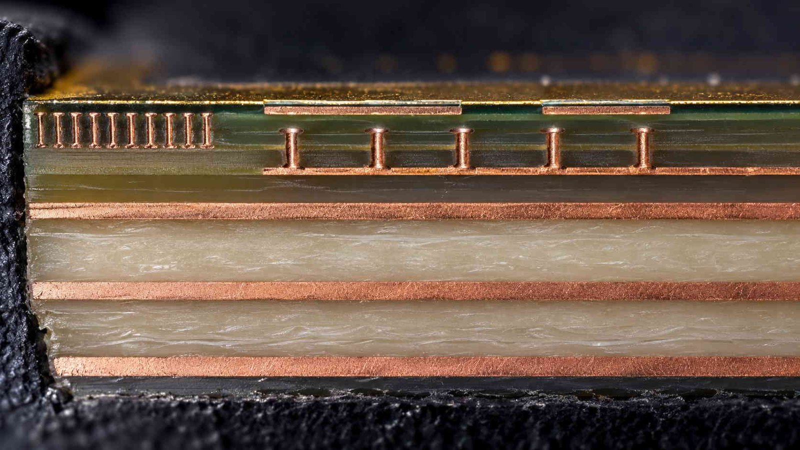
At 6 GHz a through via is a stub that resonates far above the band and is ignored. At 140 GHz the quarter-wave resonance of even a thin board's stub lands at or below the band edge, and the via becomes a radiating structure sitting in the middle of the RF path. The arithmetic is unforgiving: λg/4 at 140 GHz on a PTFE-class laminate is 0.36 mm.
| Full-length stub (PTFE-class) | First quarter-wave resonance | Verdict at 110–170 GHz |
|---|---|---|
| 0.254 mm board | 199 GHz | Clear of the band |
| 0.508 mm board | 99.5 GHz | Below the band edge — couples into it |
| 1.0 mm board | 50.5 GHz | Deep sub-band, strong re-radiation |
| 1.6 mm board | 31.6 GHz | Unusable for a D-band RF path |
A through via that passes the RF layer and continues to the far side is a stub, and its first quarter-wave resonance is c/(4·L·√εr). On a PTFE-class laminate the limit is sharp: λg/4 at 140 GHz is 0.36 mm, so the RF path tolerates a thin core only, or a backdrilled or blind/laser via that removes the stub. Note the interaction with section 3: the thin core that makes the line work is the same thin core whose thickness tolerance has to be specified. Thicker stacks belong to the digital section of the board, not to the RF path.
The verdict column reads like a stackup constraint, because it is one. A through via under an RF layer works only on a 0.254 mm-class core; anything thicker needs a backdrilled or blind/laser via that removes the stub below the RF layer. Note the interaction with section 3: the thin core that makes the stub acceptable is the same thin core whose thickness tolerance had to be tightened, and the drilling limits that make a 0.1 mm laser via reliable are set out in our high frequency PCB drilling capabilities page. Hybrid stackups resolve the conflict by putting the RF on thin low-loss cores and the digital section on thicker FR-4 sub-composites, with the ground plane between them doing the separation; the hybrid rules are in microstrip versus stripline and the connector-side transition geometry in the RF connector launch guide.
6. Solder Mask and Surface Finish: Foreign Material in the Field
Two routine materials sit inside the electric field of a D-band trace and both of them are far worse dielectrics — or conductors — than the laminate. The first is solder mask: a photoimageable epoxy with a loss tangent around 0.025, more than twenty times the laminate's. The second is the metallic finish: nickel, the barrier layer in immersion gold, with twice copper's surface resistance.
| Field fraction in the solder mask | Added loss per 10 mm | Versus laminate dielectric loss (0.18 dB) |
|---|---|---|
| 5 % | 0.41 dB | 2.2× |
| 10 % | 0.82 dB | 4.5× |
| 15 % | 1.22 dB | 6.6× |
Field-fraction estimate for a liquid photoimageable mask, εr 3.5 / tanδ 0.025, computed the same way as the laminate dielectric loss and scaled by the share of the field that sits in the mask above the trace. Even at a 5 % field fraction the mask roughly doubles the dielectric loss of the section it covers. The estimate has to be confirmed on a coupon, but the design conclusion does not wait for the coupon: at D-band the RF region is specified mask-free, and the mask opening is part of the fabrication drawing, not an afterthought.
The mask numbers are an estimate — the field fraction depends on the mask thickness and the trace geometry, and the honest confirmation is a coupon with and without mask — but even the conservative row changes the design: at a 5 % field fraction the mask doubles the dielectric loss of the section it covers, and at 10 % it costs more than the laminate itself. D-band RF regions are specified mask-free, with the opening defined on the fabrication drawing. Below 30 GHz the same mask costs hundredths of a dB and nobody opens it; the drawing-level discipline is a D-band habit, not a universal one.
The finish is a subtler version of the same problem. Current at 140 GHz occupies 0.177 µm of copper; a 2 µm nickel layer is nearly six nickel skin depths, so whatever current the finish region carries flows in nickel, at twice copper's surface resistance. The finish choice therefore belongs in the loss budget for the trace regions it touches, and the pad-type call-outs in the section 8 checklist treat it as such. Neither material is exotic — the point is that at D-band, nothing that sits in the field is electrically invisible any more.
7. What Can and Cannot Be Verified on a Coupon
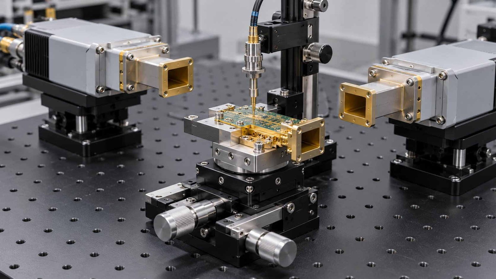
Every claim in the sections above resolves to a measurement, and the useful question at D-band is not "is it tested?" but "where does the fixture end and the board begin?". The table draws that boundary the way a fabrication line actually sees it.
| Quantity | Where it is measured | What it can and cannot tell you |
|---|---|---|
| Impedance | TDR on a dedicated coupon | Reliable. The coupon, not the board — same stackup, same lot. |
| Line geometry | Microsection and automated optical inspection | Width, etch profile, copper thickness, plating. |
| Loss trend with frequency | VNA on a coupon, to 110/145 GHz with extenders | Trend and level per centimetre; fixture extraction dominates above 110 GHz. |
| Dk on the actual lot | Coupon resonator or ring | The number the design should have used. |
| Full-board S-parameters at 140 GHz | System integrator, waveguide or probe fixture | Not a fab measurement: launch, fixture and calibration dominate. |
The honest boundary for a PCB manufacturer at D-band: impedance, geometry, loss trend and lot Dk are coupon measurements a fab can deliver with the lot. Full-board performance at 140 GHz is a system measurement that depends on the fixture as much as the board, and any supplier who quotes it as a standard deliverable is quoting something their process does not control. The coupon structures themselves — TRL/LRM geometries and connector launches — are covered in our 110–145 GHz calibration board guide, and the VNA method in the mmWave PCB VNA testing article.
The first two rows are unambiguous: TDR impedance on a coupon and microsection geometry are measurements the fab controls and delivers with the lot. The third and fourth rows are coupon measurements with caveats — a VNA with frequency extenders reaches 110 or 145 GHz routinely, but above that the fixture's own extraction dominates the error budget, so the deliverable is a loss trend and a level per centimetre, not a certified S-parameter set. The fifth row is the one that keeps programs honest: full-board performance at 140 GHz depends on the launch, the fixture and the calibration as much as on the laminate, and it belongs to the system integrator.
The practical corollary: the coupon structures have to be designed into the panel before the build, and their geometry is its own discipline — TRL and LRM line-resistor-match patterns, connector launches rated for the band, and ground return paths that survive the transition from coaxial fixture to substrate. That design work is set out in our 110–145 GHz calibration board guide, and the general VNA measurement method for millimetre-wave boards in the mmWave PCB VNA testing article. A supplier who states this boundary precisely is a better D-band partner than one who quotes the fifth row.
8. The DFM Checklist Before Gerber Release
New on this subject
- gap waveguide PCB manufacturing — pin-height stopband, board-thickness coupling and the 117 µm lid gap at D band
Nothing in this guide is exotic; every item is a line on a fabrication drawing or a purchase order, and each one traces back to a number computed above. The checklist is deliberately short — eight lines — because at D-band the expensive failures come from the ordinary items nobody escalated, not from the exotic ones everybody remembered.
| # | Drawing or PO line item | Why it is on the list |
|---|---|---|
| 1 | Core thickness tolerance for RF layers, ±5 µm or better | Dominant impedance term (section 3) |
| 2 | Etch compensation from a coupon, not a default value | Line width is 0.4 mm; ±5 µm is ±0.85 % |
| 3 | RF region mask-free; mask opening on the drawing | Mask loss rivals the laminate (section 6) |
| 4 | No full-length through vias on RF layers; blind, laser or backdrilled | λg/4 at 140 GHz is 0.36 mm (section 5) |
| 5 | Surface finish called out per pad type on RF traces | Nickel surface resistance is 2× copper at 140 GHz |
| 6 | Ground fence pitch ≤ 0.078 mm (λg/20) around RF regions | Leakage scales with the gap, and the gap is the wavelength |
| 7 | TDR coupon, loss-trend coupon and Dk coupon on the same lot | The three measurements that back sections 2–4 |
| 8 | Material lot traceability from panel to serial | Dk tolerance is a frequency error; the lot is the unit of risk |
Eight lines, all of them cheap to write into a purchase order and all of them expensive to reconstruct after a first article fails. Items 1–5 are fabrication drawing items; 6–8 belong in the purchase order and the lot documentation. A board that ships with the three coupons of item 7 has measured answers to the questions that section 7 raises.
Three questions close the review. Is the RF core thickness an explicit tolerance with a TDR coupon behind it, or an inherited default? Does any full-length via sit under an RF trace, and if the core is thicker than 0.254 mm, is the stub removed rather than tolerated? And is the mask opening for the RF region on the drawing, or is it a conversation with the fab after the first article? A board that answers those three has its loss budget, its impedance window and its via strategy under contract before the panel is imaged.
For the adjacent problems — wideband electronic-warfare front ends where the same loss logic applies an octave at a time, and the quality regime that backs these measurements — see the EW PCB wideband design guide and the RF PCB quality control inspection guide. When the design is earlier than a checklist — still choosing between laminate families or deciding where the waveguide transition lands — the PCB material comparison chart and our RF PCB manufacturer overview are the right starting points.
D-Band PCB — Frequently Asked Questions
What a PCB can and cannot do at 110–170 GHz, foil choice, solder mask, and the data a lot should ship with.
Can a PCB really carry a 140 GHz signal?
Over short distances, yes — and the honest answer includes the number. On a 0.127 mm PTFE-class laminate a 50 Ω microstrip line loses about 0.6 dB per 10 mm at 140 GHz, so a 30 mm route costs roughly 2 dB and a 100 mm route costs 6 dB. That is why D-band boards keep the RF section to a few tens of millimetres between the transition, the device and the antenna, and why longer runs move into waveguide or a quasi-optical path. The board is not the long-haul medium at these frequencies; it is the transition medium.
Why is FR-4 not an option at D-band?
The dielectric loss tangent does the damage. FR-4's tanδ of about 0.02 turns into roughly 6 dB of dielectric loss per 10 mm of 50 Ω line at 140 GHz — before the conductor contributes anything. Ten millimetres is the length of a bond pad fan-out, so there is no layout trick that makes the number survivable. FR-4 still appears on D-band assemblies, but only in the digital or mechanical sections of a hybrid stackup, below a ground plane that separates it from the RF layers.
Do I need smoother copper foil for a D-band board?
It is less decisive than most people expect. At 140 GHz the copper skin depth is 0.177 µm, and both rolled foil (about 0.8 µm roughness) and standard electrode-deposited foil (about 3 µm) are many skin depths rough, so the roughness correction saturates near a factor of two for either. The levers that actually move the loss are line width — a thicker core gives a wider 50 Ω line and cuts total loss by a third — and the surface finish on top of the trace, where nickel's surface resistance is twice copper's. Foil type is a second-order term at these frequencies, not the first-order one it is at 6 GHz.
Should solder mask cover the RF traces?
No. A liquid photoimageable mask has a loss tangent around 0.025 — more than twenty times the laminate's — and even if only 5 % of the electric field sits in the mask above the trace, it adds roughly 0.4 dB per 10 mm, which is more than the laminate's own dielectric loss. At 10 % the mask costs more than double the substrate. The standard answer at D-band is to keep the RF region mask-free, define the opening on the fabrication drawing, and confirm the field-fraction assumption on a coupon before the design is frozen.
What should a D-band PCB supplier actually deliver with a lot?
Three coupons and a statement of limits. The coupons: TDR impedance on the same stackup, a loss-trend measurement to at least 110 GHz, and a Dk measurement on the actual material lot. The statement: which quantities the fab controls — geometry, impedance, coupon-level loss — and which ones it does not, namely full-board S-parameters at 140 GHz, which belong to the system integrator's fixture. A supplier who draws that boundary precisely is easier to build a D-band program with than one who promises the unmeasurable.
Building a D-band or upper millimeter-wave board?
Send us the band, the stackup and the RF section outline. We will confirm the thin-core tolerance call-outs, the via strategy and the mask-free RF region before the layout is frozen, and quote fabrication with TDR, loss-trend and Dk coupons built from the same lot.
Contact Us → WhatsApp: +86 137 6047 3650Request a PCB Quote
Upload your Gerber ZIP file and project requirements. Our engineering team will review your PCB material, stackup, impedance needs, surface finish, and production quantity before quoting.
Please prepare:
- Gerber files in ZIP format
- PCB material or stackup requirements
- Controlled impedance notes if available
- Prototype or batch production quantity