
Rogers RO4835 PCB: Ceramic-Filled Laminate for Antennas and High-Power RF
RO4835 PCB design data: process Dk 3.48 and design Dk 3.66, dissipation factor 0.0037 at 10 GHz, Tg above 280 °C, and the thickness, copper and lamination options that decide an antenna or high-power RF build.
Home » Antenna PCB » Rogers RO4835 PCB: Ceramic-Filled Laminate for Antennas and High-Power RF
Table of Contents
RO4835 PCB is a circuit board built on the ceramic-filled hydrocarbon laminate supplied in the RO4000-series RO4835 group. The material pairs a thermoset hydrocarbon resin with ceramic filler, which is what produces a stable dielectric constant of 3.48 and a dissipation factor of 0.0037 at 10 GHz while keeping the board processable on standard epoxy/glass fabrication lines.
That combination is why the grade turns up on antenna panels, phased-array feed networks, point-to-point microwave links and RF power amplifiers: designs where the electrical performance has to hold over temperature and over years in the field, and where the fabrication route still has to be economical at volume.
This page collects the published data-sheet values for RO4835, shows which dielectric constant belongs in an impedance calculation, and sets out the thickness, copper and lamination options that decide what can actually be built. Material families grouped by application are listed in our high frequency PCB materials section, and the grade-by-grade parameter view sits in the Rogers materials pages.
1. What Is RO4835 PCB?
RO4835 belongs to the class of laminates in which a hydrocarbon resin is loaded with ceramic filler. The filler is what makes the dielectric constant stable rather than something that drifts with frequency and temperature, and the hydrocarbon resin is what makes the material a thermoset that can be pressed and drilled on equipment already set up for epoxy/glass boards.
Practically, that means a board designer gets two things at once. The electrical behaviour is closer to a specialist microwave substrate than to FR-4, with a loss figure in the 0.0037 range at 10 GHz. At the same time the fabrication route stays short: no hole-wall activation step before plating, lead-free assembly compatible, and a lamination sequence that does not consume the board thickness in process risk.
The third property that matters over a product life is stability. A thermoset substrate oxidises slowly at temperature, and oxidation raises both Dk and Df. The grade is published as delivering about ten times the oxidation resistance of typical thermoset microwave materials, which is the difference between an antenna that is still tuned in year five and one that has drifted.
2. RO4835 Laminate Properties: The Datasheet Values
Everything in the table below is a published typical value at the test condition shown in the last column. Values that could not be confirmed in the data sheet are not listed, and nothing in this page is estimated.
| Category | Property | Typical value | Test condition |
|---|---|---|---|
| Electrical | Dielectric constant (process) | 3.48 ± 0.05 | 10 GHz, 23 °C |
| Electrical | Dielectric constant (design) | 3.66 | 8–40 GHz, differential phase length |
| Electrical | Dissipation factor | 0.0037 | 10 GHz, 23 °C |
| Electrical | Thermal coefficient of Dk | +50 ppm/°C | −50 °C to 150 °C |
| Electrical | Volume resistivity | 5 × 10⁸ MΩ·cm | Condition A |
| Electrical | Surface resistivity | 7 × 10⁸ MΩ | — |
| Electrical | Dielectric strength | 30.2 kV/mm (755 V/mil) | — |
| Physical | Flammability | UL 94 V-0 | — |
| Physical | Moisture absorption | 0.05 % | 50 °C, 48 h |
| Physical | Density | 1.92 g/cm³ | 23 °C |
| Physical | Lead-free process | Compatible | — |
| Physical | CAF resistance | Resistant | — |
Published typical values for the laminate, at the test condition given in the last column. Specification limits for a specific lot come from the material certificate, not from this table.
Read the two Dk rows separately, because they answer different questions. The process value of 3.48 is the material specification; the design value of 3.66 is what a simulation should use. That distinction is the subject of the next section.
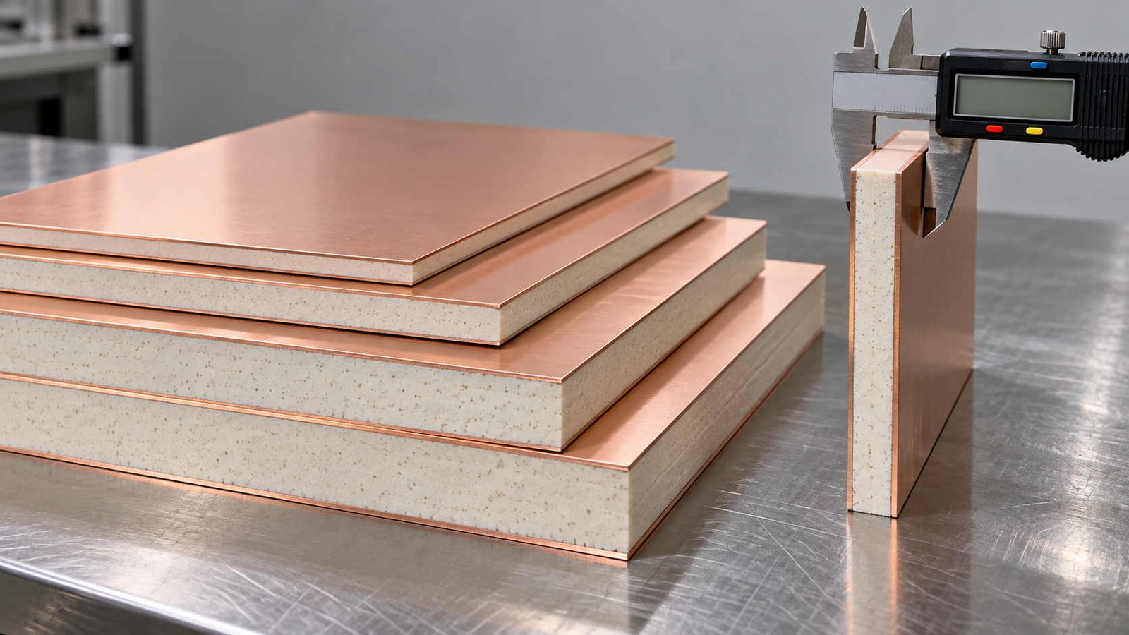
3. Process Dk vs Design Dk: Which Number Goes Into the Calculation
The single most common error on a first RO4835 design is to run the impedance calculation with the process dielectric constant, then find that measured impedance is several percent below target on the coupon. The two numbers are not alternative readings of the same quantity; they describe different things.
The process Dk is a material property measured on a clamped stripline fixture. The design Dk is an average taken from several tested lots and on the most common thicknesses, and it is higher, because a real trace geometry does not load the field the way the test fixture does. A field solver wants the design value.
| Number | Value | What it is used for |
|---|---|---|
| Process Dk | 3.48 ± 0.05 at 10 GHz, 23 °C | The material figure. It is what an incoming inspection measures and what makes one lot comparable with the next. |
| Design Dk | 3.66, quoted over 8–40 GHz | The number that goes into a field solver. It is an average taken on the most common thicknesses, and it is higher than the process value because a real trace geometry does not load the field the way a clamped stripline test fixture does. |
| Process Dk on the 0.10 mm gauge | 3.33 ± 0.05 at 10 GHz | The thin gauge carries its own published process value. A thin-core design should be released against that figure rather than the general one. |
| Thermal coefficient of Dk | +50 ppm/°C, −50 °C to 150 °C | The drift term in a phase or resonant-frequency budget across the operating temperature range. |
The most common error in a first RO4835 design is to run the impedance calculation with the process Dk and then wonder why measured impedance comes in low. The process value describes the material; the design value describes the trace. For the wider impedance picture see our article on controlled impedance RF PCB.
How Dk and Df translate into loss, impedance and phase on a finished board is the subject of a separate article on how Dk and Df affect high frequency PCB performance. On a ceramic-filled laminate there is one further check: the tolerance is stated as ±0.05 on the process value, and a design that depends on absolute frequency accuracy should budget that window rather than assume a nominal Dk.
4. Dielectric Thickness, Panel Size and Copper Options
Thickness and copper weight are not packaging choices on a high-frequency board — they set the trace width that produces a target impedance, and they set how much of the loss is dielectric and how much is conductor.
| Item | Standard offering | Note |
|---|---|---|
| Dielectric thickness | 0.10 mm (0.004 in) ± 0.018 mm | Thin gauge; published with its own process Dk of 3.33 ± 0.05. |
| Dielectric thickness | 0.17 mm (0.0066 in) ± 0.018 mm | Common thin core for millimetre-wave work. |
| Dielectric thickness | 0.25 mm (0.010 in) ± 0.025 mm | Frequently used for 50 Ω microstrip lines. |
| Dielectric thickness | 0.51 mm (0.020 in) ± 0.038 mm | Standard RF core thickness. |
| Dielectric thickness | 0.76 mm (0.030 in) ± 0.051 mm | Thicker core for wider traces and lower loss per unit length. |
| Dielectric thickness | 1.52 mm (0.060 in) ± 0.102 mm | Thickest standard gauge. |
| Panel size | 305 × 457 / 610 × 457 / 610 × 915 / 1219 × 915 mm | Panel choice drives utilisation and how many array elements fit per panel. |
| Standard cladding | Electrodeposited copper, 1/2 oz (18 µm) and 1 oz (35 µm) | Copper weight sets conductor loss and current capacity. |
| Flammability | UL 94 V-0 | Required in many sealed automotive and telecom assemblies. |
Thickness availability is the constraint to check first on a millimetre-wave design: if the gauge the layout was dimensioned for is not offered, the design is re-dimensioned rather than simply rebuilt on a different core. Non-standard configurations can be requested.
Note the tolerance column. A ±0.102 mm window on the 1.52 mm gauge is a wide number in percentage terms, and on a design where thickness tolerance feeds directly into impedance it is worth checking whether a tighter construction is needed. The thinner gauges carry tighter windows for exactly that reason.
5. Antenna and RF Applications of RO4835
The published application set for the laminate is an antenna and power set: automotive radar and sensors, point-to-point microwave, power amplifiers, phased-array radar and RF components. Rather than repeat a grade name, it is more useful to match each application to the board requirement it imposes and then to the one or two data-sheet figures that answer it.
| Application | What the board has to do | Which property carries it |
|---|---|---|
| Antenna panels and element substrates | Hold element and feed dimensions repeatably across a large panel and across production lots. | Tight Dk tolerance (±0.05), design Dk 3.66, dimensional stability <0.5 mm/m |
| Phased-array radar | Keep a corporate feed network phase-matched across many elements and many boards. | Dk tolerance lot to lot, low in-plane CTE (10 / 12 ppm/°C) |
| Automotive radar and sensors | Run phase-stable feed lines in a sealed module that gets hot and stays hot. | Df 0.0037, TCDk +50 ppm/°C, Tg >280 °C |
| RF power amplifiers | Get heat out of the device pad and through the board without delamination. | Thermal conductivity 0.66 W/(m·K), Td 390 °C, low Z-axis CTE |
| Point-to-point microwave | Hold insertion loss over a fixed link length, year after year. | Df 0.0037 plus oxidation resistance, moisture absorption 0.05 % |
| RF components and filters | Land on the same resonant frequency on the second lot as on the first. | Design Dk 3.66 with the ±0.05 process window |
The list is the application set published for the laminate. What the three columns are really doing is matching a board requirement to the one or two datasheet figures that decide it, so that a specification can be written around the parameters that matter instead of around a grade name.
Two of these applications are treated in more detail elsewhere on this site. Antenna substrate choices are compared in PCB materials for antenna applications, and array work — where Dk tolerance across a panel matters more than absolute Dk — is covered in the phased array PCB review. Fabrication of antenna boards, including element tolerance control, is described on our antenna PCB product page.
6. Thermal Behaviour at High Power and High Duty Cycle
On a receive-only board the thermal columns of a datasheet can be treated as background. On a transmit board or an amplifier board they are the specification. Heat has to leave the device through the copper, spread into the ground plane, and then either spread laterally through the laminate or be carried out through a via array.
| Parameter | Typical value | What it decides on the board |
|---|---|---|
| Decomposition temperature (Td) | 390 °C | Margin above the peak of a lead-free reflow profile. |
| Glass transition temperature (Tg) | >280 °C | Whether expansion behaviour stays constant through several reflow passes and at high ambient temperature. |
| CTE, Z axis | 31 ppm/°C | Barrel strain in plated through-holes through thermal cycling on multilayer and thick builds. |
| CTE, X and Y axes | 10 / 12 ppm/°C | Registration and element-dimension drift through lamination and assembly. |
| Thermal conductivity | 0.66 W/(m·K) at 80 °C | How quickly heat spreads away from a device pad or a high duty-cycle trace into the ground plane. |
| Dimensional stability (x, y) | <0.5 mm/m after etch | Whether etched element, stub and filter dimensions stay inside tolerance after processing. |
| Copper peel strength | 0.88 N/mm (5.0 pli) | Foil adhesion after solder float — the figure behind lifted-pad and delamination risk. |
Thermal and mechanical parameters do not appear in an electrical simulation, which is why they are the columns most often left out of a specification and the ones that decide whether a board survives assembly and field life. On a high duty-cycle transmitter the thermal conductivity of the laminate sets how much of the device heat has to be removed through vias rather than spread through the board.
The two figures that decide the outcome are thermal conductivity, which sets how fast heat spreads inside the laminate, and the Z-axis coefficient of thermal expansion, which sets how much the plated barrel is strained each time the board cycles. A design that runs hot also cycles between room and operating temperature repeatedly, which is where a low Z-axis figure earns its place. Thermal design for a high-power amplifier stage, including via-array density and ground-pad void control, is worked through in our guide to thermal design for RF power amplifier PCBs.
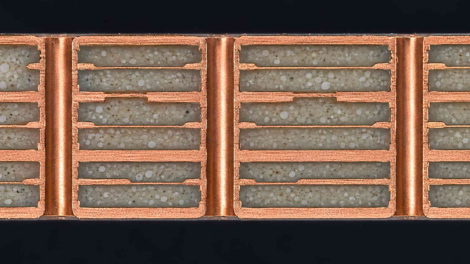
7. Long-Term Stability: Oxidation, Moisture and Dimensional Drift
A ceramic-filled hydrocarbon laminate is a thermoset, and thermosets oxidise. The rate is slow, but the consequence is directional: Dk and Df both creep upward as the resin oxidises, and on a narrowband element or a filter that creep is a frequency shift. The published oxidation resistance of the grade — around ten times that of typical thermoset microwave materials — is aimed squarely at that mechanism.
| Property | Value | Why it matters over field life |
|---|---|---|
| Oxidation resistance | 10× that of typical thermoset microwave materials | An oxidising thermoset substrate drifts upward in Dk and Df over years at temperature. Slower oxidation means the tuning set at design time stays closer to the tuning in year five. |
| Moisture absorption | 0.05 % at 50 °C / 48 h | Absorbed water raises both Dk and loss. A low figure keeps the resonant frequency of a narrowband structure stable in humid or condensing installations. |
| CAF resistance | Resistant | Limits conductive anodic filament growth between closely spaced plated holes, which is a long-term failure mode on dense multilayer boards. |
| Dimensional stability | <0.5 mm/m after etch | Less movement between lamination, etching and reflow means etched element dimensions land closer to the drawn dimensions. |
| Lead-free compatibility | Compatible, no blistering or delamination | The board survives the reflow profile the assembly house actually runs. |
These are the figures that separate a laminate chosen for one prototype from a laminate chosen for a production programme. None of them appears in a datasheet headline, and all of them are the reason a high-reliability RF board stays inside its specification late in life.
Moisture works in the same direction as oxidation, and faster. Water absorbed into the substrate raises both the dielectric constant and the loss, so the moisture absorption figure belongs in the same specification discussion as Dk and Df whenever the equipment is installed outdoors, in a marine environment or in anything that is not hermetically sealed.
8. Manufacturing RO4835 Boards: What to Send and What We Check
The last thing to settle before quoting is which of the design assumptions the factory can actually hold. The table below is the list we work through on an RF build.
| Item | What we hold or need | Why it decides the build |
|---|---|---|
| Standard dielectric thicknesses | 0.10 / 0.17 / 0.25 / 0.51 / 0.76 / 1.52 mm | Sets the trace width that gives a target impedance at a given copper weight. |
| Standard cladding | ED copper 1/2 oz (18 µm) and 1 oz (35 µm) | Conductor loss and current capacity. Above about 30 GHz, foil surface roughness becomes a larger loss term than the dielectric. |
| Lamination route | Thermoset laminate processed on standard epoxy/glass lines, lead-free compatible | No hole-wall activation step is needed, so the process flow stays short and the lamination cycle count is not the limiting factor it is on PTFE builds. |
| Surface finish | ENIG, immersion silver, immersion tin, OSP | Solderability and launch loss. Hot-air solder levelling is avoided on high-frequency assemblies. |
| Minimum drill | 0.20 mm mechanical, 0.10 mm laser | Decides whether the via density the layout needs is buildable at the pitch the design assumes. |
| Impedance verification | Coupon TDR measured against the design Dk assumption | Confirms the number used in simulation against the lot that was actually laminated. |
| Files and data we need | Gerbers + NC drill, stackup, material and thickness, copper weight, surface finish, impedance targets, IPC Class, quantity | Every one of these changes the quote, and a missing item is what causes a design to come back after DFM. |
The point of listing these together is that on a high-frequency build the material decision and the process decision are not separable: a thickness that is not offered, or a drill pitch below the process floor, invalidates a layout that is electrically correct.
The broader fabrication sequence — drilling parameters, dimensional tolerance and surface finish on RF laminates — is described in our Rogers PCB manufacturing requirements note and in the high frequency PCB drilling capabilities summary. Send the Gerbers with the stackup and the impedance targets and we will confirm the thickness and copper combination before anything is cut.
RO4835 PCB — Frequently Asked Questions
The datasheet values, which one goes into an impedance calculation, and what the grade is specified for.
What is RO4835 PCB?
RO4835 PCB is a printed circuit board built on the ceramic-filled hydrocarbon laminate supplied in the RO4000-series RO4835 group. The resin is a thermoset hydrocarbon system loaded with ceramic filler, which produces a process dielectric constant of 3.48 ± 0.05 at 10 GHz, a dissipation factor of 0.0037 at 10 GHz and a design dielectric constant of 3.66 quoted over 8 to 40 GHz. The glass transition temperature is above 280 °C, the decomposition temperature is 390 °C, and the laminate is rated UL 94 V-0. It is processed with epoxy/glass fabrication techniques, including lead-free assembly, which is why the same material appears on antenna panels, phased-array feed networks, automotive radar modules and RF power amplifiers rather than only on low-volume specialist builds.
Which dielectric constant should be used for an impedance calculation on RO4835?
The design Dk of 3.66 is the figure to simulate with, because it is the average value measured across the most common thicknesses over 8 to 40 GHz range. The process Dk of 3.48 ± 0.05 at 10 GHz is the figure quoted for material specification and lot-to-lot comparison. The two are not interchangeable: a field solver run with the process value understates the loading that a real trace geometry applies, and measured impedance then comes in below target. There is one further case to watch. The 0.10 mm gauge is published with its own process Dk of 3.33 ± 0.05, so a thin-core design should be checked against that figure rather than against the general one.
What dielectric thicknesses and copper weights are available on RO4835?
Standard dielectric thicknesses are 0.10, 0.17, 0.25, 0.51, 0.76 and 1.52 mm, with published tolerances of ±0.018, ±0.018, ±0.025, ±0.038, ±0.051 and ±0.102 mm respectively. Standard cladding is electrodeposited copper at 1/2 oz (18 µm) or 1 oz (35 µm), on panel sizes from 305 × 457 mm up to 1219 × 915 mm. Reverse-treated low-roughness foil is available in the RO4000 series for designs where conductor loss dominates above roughly 30 GHz. Thickness availability is the constraint to check first on a millimetre-wave design, because a gauge that is not offered forces the layout to be re-dimensioned rather than rebuilt.
Why is RO4835 specified for antenna boards and high-power RF?
Two groups of properties. Electrically, the dissipation factor of 0.0037 at 10 GHz keeps insertion loss down along long feed networks, and the ±0.05 process tolerance keeps element and filter dimensions repeatable from lot to lot. Thermally and mechanically, a decomposition temperature of 390 °C, a glass transition temperature above 280 °C and low in-plane expansion keep a multilayer antenna panel dimensionally stable through lamination and lead-free reflow, while the 31 ppm/°C Z-axis figure limits barrel strain in plated through-holes. Because oxidised thermoset substrates drift upward in Dk and Df over time, the published oxidation resistance of the grade is the part that keeps the antenna tuned late in the product's life.
Building an RO4835 antenna or power board?
Send us the band, the dielectric thickness you have in mind and the copper weight. We will confirm which thickness is available in the gauge your layout needs, agree the Dk figure to be used for the impedance target, then quote fabrication with coupon TDR data on the lot we actually build from.
Contact Us → WhatsApp: +86 137 6047 3650Request a PCB Quote
Upload your Gerber ZIP file and project requirements. Our engineering team will review your PCB material, stackup, impedance needs, surface finish, and production quantity before quoting.
Please prepare:
- Gerber files in ZIP format
- PCB material or stackup requirements
- Controlled impedance notes if available
- Prototype or batch production quantity