High Frequency PCB Prototype Manufacturer — 5–10 Day Turnaround
Riching PCB manufactures RF antenna PCB — single patch elements, antenna arrays, phased arrays and feed networks — on Rogers RO3003, RT5880 and RO4350B. ENIG surface finish standard for dimensional accuracy. RO3003 ±0.04 Dk tolerance in stock. In-house plasma activation. 7–10 day prototype. No MOQ.
Home » antenna array PCB » RF Antenna PCB Manufacturer — Patch & Array Antennas In Stock
Table of Contents
ENIG
standard finish
dimensional accuracy
±0.04
Dk tolerance
RO3003 in stock
2.5mil
min trace/space
dense feed networks
7–10
day prototype
no MOQ
Antenna Types and Material Selection
Antenna PCB design requirements vary significantly by type and frequency. The table below maps common antenna types to recommended materials and dedicated pages with application-specific specifications.
| Antenna Type | Frequency Range | Recommended Material | Dedicated Page |
|---|---|---|---|
| Single patch element | 1–40 GHz | RO4350B or RO3003 depending on freq | RF PCB Manufacturer → |
| Patch antenna array (76–77GHz) | 76–81 GHz | RO3003 0.127mm | 77GHz Radar PCB Manufacturer → |
| Phased array / beamforming | X / Ku / Ka band | RO3003, tight Dk uniformity | Phased Array PCB Manufacturer → |
| Ka-band satcom array | 26.5–40 GHz | RO3003 / RT5880 | Ka-Band PCB Manufacturer → |
| Wideband ESM/EW antenna | 2–18 GHz | RT5880 | EW PCB Manufacturer → |
| Feed network / power divider | Varies | Match to array material | Controlled Impedance PCB Manufacturer → |
Precision Requirements for Antenna PCB
Unlike general RF circuits, antenna elements are resonant structures — their physical dimensions directly determine operating frequency. Small variations in etch tolerance, Dk, or surface flatness shift the resonant frequency of every element on the board.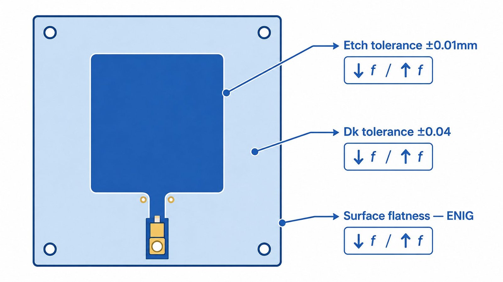
| Factor | Impact on Antenna Element | Riching PCB Control |
|---|---|---|
| Surface flatness | Patch dimensions vary with surface warp — shifts resonant frequency | ENIG standard — flat surface for dimensional accuracy |
| Etch tolerance | Patch edge variation shifts resonant frequency | ±0.01mm etch tolerance, ±20% on fine features |
| Dk tolerance | Element resonant frequency depends on Dk | RO3003 ±0.04 — tightest in PTFE range |
| Via fence placement | Affects element isolation and pattern shape | 0.4mm center-to-center, consistent across panel |
| Copper weight uniformity | Affects trace width and element edge definition | 0.5oz–1oz controlled per layer |
For array designs where element-to-element consistency matters — not just single-element accuracy — see phased array PCB manufacturer for panel-level Dk uniformity controls.
Feed Network and Via Fence Design
- Corporate feed networks: impedance-matched power dividers, see controlled impedance PCB manufacturerfor ±5% TDR option
- Via fence isolation between elements — design rules in RF via fence PCB
- Min trace/space 2.5mil/2.5mil — supports dense feed network routing for large arrays
- Min drill 0.2mm mechanical, 0.1mm laser — for via fence and feed network vias
Materials In Stock for Antenna PCB
- Rogers RO3003— 0.127 / 0.254mm, Dk 3.0 ±0.04, standard for 77GHz and Ka-band patch arrays
- Rogers RT5880— 6 thicknesses in stock, lowest Df for wideband EW antennas
- Rogers RO4350B / RO4003C— for antennas below 18GHz, FR4-compatible process
How to Order
- WhatsApp: +86 13760473650
- Send: Gerber zip + NC drill + stackup drawing
- Specify: material grade + thickness, target resonant frequency, impedance for feed network
- DFM review confirms patch dimensions vs production Dk: 4–8 hours
- No MOQ. From 1 board.
RF Antenna PCB Manufacturer — Shenzhen Direct Factory
Patch & Array Antennas · RO3003 RT5880 In Stock
ENIG Standard · ±0.04 Dk · 7–10 Day Prototype
Send Gerber + stackup drawing. DFM review within 4–8 hours.
Specify material, thickness and target resonant frequency.
DFM review within 4–8 hours
Request a PCB Quote
Upload your Gerber ZIP file and project requirements. Our engineering team will review your PCB material, stackup, impedance needs, surface finish, and production quantity before quoting.
Please prepare:
- Gerber files in ZIP format
- PCB material or stackup requirements
- Controlled impedance notes if available
- Prototype or batch production quantity