
OpenVPX RF PCB: Designing SOSA-Aligned 3U and 6U RF Platform Boards
OpenVPX RF PCB manufacturing for SOSA-aligned 3U and 6U boards: VITA 67 launches, cavity resonance, backdrill stubs, rail IR drop and the thermal path to the chassis.
Home » Electronic Warfare PCB » OpenVPX RF PCB: Designing SOSA-Aligned 3U and 6U RF Platform Boards
Table of Contents
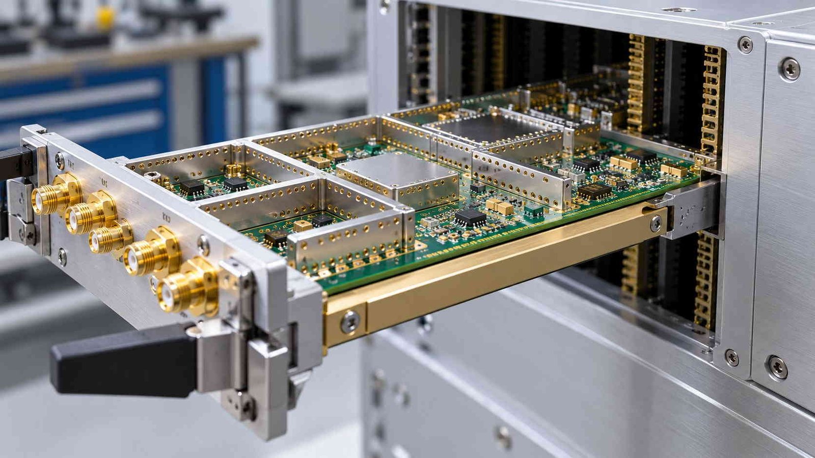
Open platforms have reached the RF module. European Microwave Week 2026 showcases — Planar Monolithics' SOSA-aligned 0.1–18 GHz transceiver in a 3U OpenVPX, 10-HP format with VITA 67 RF connectivity, next to a 0.1–40 GHz I/Q vector modulator — mark where electronic-warfare hardware is going: modular, re-cardable, ultra-wideband, and built on boards whose every millimetre is budgeted. The sensor-open-systems architecture (SOSA) alignment is not a component specification; it is a set of obligations the PCB has to carry.
Those obligations are computable, and this page computes them from one stated model: what a 3U envelope forces on section planning, why the VITA 67 launch is a tuned structure at 18 GHz, how compartment width trades against cavity resonance, where backdrill stubs land in a 2.4–3.2 mm stack, what a PA rail loses in IR drop, which term actually dominates the thermal path to the chassis, and how much phase error a material lot can inject into a coherent array. Every figure is computed; the assumptions are stated where they are used.
The wideband front-end design side — filter choices, gain planning, dynamic range — is treated in our EW PCB wideband design guide. This page is about the platform board those designs land on: 3U and 6U, VITA 67 on the panel, wedge locks on the edge.
1. What a SOSA-Aligned Envelope Forces on the Board
The form factor is fixed; everything else competes for it. The table translates the OpenVPX classes into the rectangle a fabricator actually sees.
| Form factor | Board envelope (VITA 48 class) | Board area | Front-panel pitch | What the envelope forces |
|---|---|---|---|---|
| 3U | 100 × 160 mm | 16,000 mm² | 3 HP = 30.5 mm / 10 HP = 203 mm | RF and digital share a very small rectangle |
| 6U | 233.35 × 160 mm | 37,336 mm² | same HP grid | More compartments, same edge space |
Standard OpenVPX envelopes — the layer counts, thicknesses and connector apertures vary per build, but the rectangle is fixed. The 3U row is the design pressure point: a 100 × 160 mm board has to hold the RF chain, the FPGA-side digital, the power entry and the shielding walls at once, which is why compartment planning (section 3) happens at stackup review, not at layout. The HP pitch also fixes where VITA 67 apertures can sit relative to the wedge-lock edge.
On a 3U board the RF chain, the FPGA-side digital, the power entry and the shielding walls share 16,000 mm², and the HP pitch fixes where VITA 67 apertures can sit relative to the wedge-lock edge. That scarcity is why SOSA platform boards are decided at stackup review — compartment map, RF layer assignment, rail copper, thermal path — long before layout. By the time the CAD file exists, the expensive decisions have already been made; the fabricator's job is to make sure they were made with the numbers in the sections below.
The 6U class relaxes area but not discipline: 233 mm of edge length raises its own questions about slot stiffness, connector alignment and the thermal wedge, and the layer count typically rises with it — which pulls backdrill arithmetic (section 4) into every revision.
2. VITA 67 Launches and the Electrical Scale of the First Millimetre
The VITA 67 aperture is where the cable world ends and the board begins, and the transition owns a disproportionate share of the channel budget because of one number: the in-board wavelength. The table converts it for a hydrocarbon-class RF layer.
| Frequency (hydrocarbon-class RF layer, εr 3.48) | In-medium wavelength λg | Phase per millimetre | First-millimetre verdict |
|---|---|---|---|
| 6 GHz | 26.8 mm | 13.4°/mm | Launch parasitics are a trim term |
| 18 GHz | 8.93 mm | 40.3°/mm | The launch is a tuned structure |
| 40 GHz | 4.02 mm | 89.6°/mm | Pads, anti-pads and stubs are the circuit |
Computed for a hydrocarbon-class RF layer (εr 3.48) — the common SOSA transceiver band runs to 18 GHz, with the newest I/Q modulator parts reaching 40 GHz. The last column is the point: at 18 GHz one millimetre of unplanned geometry is 40 degrees, so the VITA 67 aperture, the pad transition and the first via are circuit elements with values, not mechanical details. Launch geometry — pad size, anti-pad diameter, ground return placement — is treated in our PCB-to-RF-connector launch guide.
At 18 GHz the first millimetre past the connector is worth 40 degrees of phase, so pad size, anti-pad diameter, ground return placement and the first via are tuned elements — they belong on the fabrication drawing with tolerances, not in a layout default. At 40 GHz, the reach of the newest I/Q modulator parts, a millimetre is nearly a quarter wavelength and the launch is the circuit. The transition design — pad geometry, anti-pad sizing, return-via placement and the launch de-embedding used to verify them — is set out in our RF connector launch guide, and the measurement side in the RF/mmWave test fixture guide.
3. Shielding Compartments Are a Circuit Decision
Every metal wall on a SOSA board encloses a cavity, and every cavity is a waveguide whose cutoff frequency is set by its width. The table is the whole argument.
| Compartment width a (air cavity) | TE10 cutoff c/2a | Usable bands | Design consequence |
|---|---|---|---|
| 4 mm | 37.5 GHz | Everything below | Costly in area; used near 40 GHz sections |
| 6 mm | 25.0 GHz | Below ~24 GHz | Practical for 18 GHz RF chains |
| 8 mm | 18.7 GHz | At the 18 GHz band edge | Last comfortable width for an 18 GHz chain |
| 10 mm | 15.0 GHz | Below 15 GHz only | Resonates inside an 18 GHz band |
| 15 mm | 10.0 GHz | Below 10 GHz only | Needs internal walls or absorber |
Dominant rectangular-cavity cutoff, fc = c/2a for an air-filled compartment. A compartment wider than c/2f_max supports propagation at the top of the band: energy leaks between sections, filters pull each other, and isolation measured on the bench never reproduces. For an 18 GHz chain the wall arithmetic gives an 8.3 mm ceiling on compartment width — the compartment map is therefore a circuit decision made with the RF team at stackup review, not a mechanical partition drawn at layout. Wider sections need internal walls, fenced apertures or absorber, each of which costs area the 3U envelope does not have.
The 8 mm row is the one to remember: for an 18 GHz chain it is the last comfortable compartment width, and anything wider either resonates in-band or has to buy isolation back with internal walls, fenced apertures or absorber — all of which spend area the 3U envelope does not have. This is why the compartment map is drawn with the RF team at stackup review, sized by cutoff arithmetic, and why a fabricator who can hold fence-via pitch and wall registration across a 233 mm 6U board is part of the design conversation, not just the quote.
The same logic scales below: ground fences and via walls around each RF section are the small-scale version of the compartment argument, and their pitch discipline is treated in the controlled impedance RF PCB guide. Where the chain pushes past 18 GHz, the budget tightens again — the losses are computed the same way as any wideband front end, in the EW wideband guide.
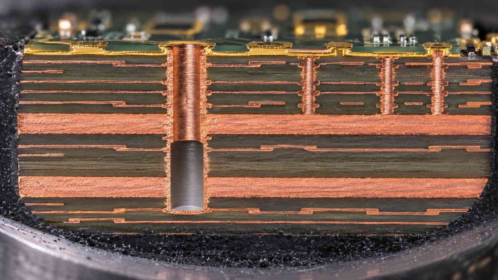
4. Backdrilling and the Layer Architecture of a 2.4–3.2 mm Board
VPX boards are thick because they carry power and stiffness as well as signal, and thickness is where stubs live. The arithmetic for a hydrocarbon-class RF layer:
| Residual stub (εr 3.48) | First λ/4 resonance | Verdict vs 18 GHz / 40 GHz chains |
|---|---|---|
| 1.0 mm | 40.2 GHz | Clear of both |
| 2.23 mm | 18 GHz | At the band edge — couples in |
| 3.2 mm un-backdrilled through hole | 12.6 GHz | Inside the band — unusable on an RF path |
f = c/(4·L·√εr). A 2.4–3.2 mm VPX board puts every un-backdrilled through via into or near the 18 GHz band, and the 40 GHz modulator sections push the residual-stub ceiling to about 1.0 mm. Backdrill depth on a board that is already 2.4–3.2 mm thick is a measured dimension — microsection or x-ray per panel — and the aspect ratio (8:1 at 2.4 mm with a 0.3 mm drill, 10.7:1 at 3.2 mm) has to be reviewed against plating capability at the same stackup review. The method is set out in our back drill PCB guide.
The verdict column reads like an architecture constraint because it is one: RF paths on a VPX board are backdrilled or blind/laser by design, with the residual stub specified as a dimension and verified by microsection or x-ray per panel. The aspect ratio rides along in the same review — 8:1 at 2.4 mm with a 0.3 mm drill, 10.7:1 at 3.2 mm — and plating capability on hydrocarbon-class materials is part of that conversation. The method and tolerances are set out in our back drill PCB guide and the high frequency PCB drilling capabilities page.
5. Power Rails: IR Drop Is a Copper-Weight Decision
A SOSA transceiver or PA module moves serious current at low voltage, and the rail is pure series loss in front of the amplifier. The table sizes the problem for a representative route.
| Rail copper (L = 100 mm, w = 2 mm) | Resistance | @ 5 A | @ 10 A |
|---|---|---|---|
| 1 oz (35 µm) | 24.0 mΩ | 0.12 V / 0.6 W | 0.24 V / 2.4 W |
| 2 oz (70 µm) | 12.0 mΩ | 0.06 V / 0.3 W | 0.12 V / 1.2 W |
| 3 oz (105 µm) | 8.0 mΩ | 0.04 V / 0.2 W | 0.08 V / 0.8 W |
R = ρ·L/(w·t) at 20 °C; hot-rail resistance is higher. A 150 W-class PA module draws tens of amperes at 28–40 V drain bias, and on a 100 mm route an ordinary 1 oz rail turns that into a quarter-volt sag plus 2.4 W of rail heating — before the PA itself contributes. Widening the rail to 5 mm recovers most of it (10 mΩ, 0.10 V at 10 A); doubling copper weight recovers the rest and halves the rail self-heating. Both belong in the stackup decision, not in a copper-pour afterthought, and the drain rail route length is part of the RF power budget.
Two levers, both decided at stackup review: width and copper weight. Widening the rail to 5 mm recovers most of the drop at 1 oz; moving the rail to 2 oz or 3 oz recovers the rest and halves the rail's own heating — which matters because the rail heats the board that is already trying to export the PA's dissipation. On GaN modules the drain rail route length is part of the RF power budget, and the mixed RF/digital/power partitioning that keeps the rail out of the RF compartments is treated in our mixed-signal high-speed design overview.
6. The Thermal Path to the Chassis: The Pour, Not the Vias
High-power SOSA modules move device heat to the wedge-lock edge through a chain: the die pad, the board pour, the thermal via array, the internal plane, the wedge locks. Most designs over-invest in the middle of that chain. The table shows why.
| Thermal element (1.6 mm board, 0.3 mm via / 25 µm wall) | Thermal resistance | Share of the path |
|---|---|---|
| Single thermal via | 174 K/W | — |
| 25-via array (parallel) | 7.0 K/W | Minor term |
| Spreading in 1 oz copper pour | 26.8 K/W | Dominant term |
| Spreading in 3 oz copper | 8.9 K/W | Halved twice |
Per-via conduction R = L/(k·A_wall), k = 390 W/mK; spreading R = ln(r2/r1)/(2π·k·t) for a 10:1 spread ratio. The counterintuitive result: the via array everyone counts is not the bottleneck — the thin copper pour it lands on is. A 10 W device on 25 vias into a 1 oz pour sees roughly 338 °C of rise before any interface or wedge-lock resistance; the same array on a 3 oz pour sees about 159 °C. That is why high-power SOSA modules specify heavy copper planes, copper coins under flanged PA devices, and a continuous low-resistance path to the wedge-lock edge — and why the coin/pour copper weight is a thermal decision made at stackup review. The chassis-side regime is treated in our massive MIMO thermal guide.
The via array — the element everyone counts — is a minor term: 25 vias in parallel are 7 K/W. The thin copper pour they land on is the bottleneck: at 1 oz, spreading alone is nearly 27 K/W, four times the array. That single number reorders the stackup review: specify the pour weight and any copper coin under flanged devices with the thermal path as the requirement, size the via array to match, and keep the path continuous to the wedge-lock edge. The chassis-side regime — conduction cooling, wedge-lock interfaces, altitude derating — is treated in our massive MIMO thermal guide.
7. Phase Matching and Channel-to-Channel Consistency
Multi-channel SOSA arrays — CRPA, direction finding, multi-beam — are coherent structures: the channels have to track in phase, and on a 160 mm 6U path the raw phase is enormous. The table shows what actually moves it.
| Channel parameter (160 mm path, εr 3.48, 18 GHz) | Phase error | Where it comes from |
|---|---|---|
| Total phase of the path | 6,452° | — |
| Dk lot tolerance ±0.02 | ±18.5° | Material lot |
| Length difference ±0.25 mm | ±10.1° | Serpentine and etch |
| Length difference ±0.10 mm | ±4.0° | Tight, coupon-verified matching |
Phase = 360·L·√εr·f/c. Multi-channel SOSA arrays — CRPA, direction finding, multi-beam — need channel-to-channel phase tracked to a few degrees, and the table shows the two terms that dominate: the material lot and the length match. A ±0.02 Dk lot swing moves an 18 GHz channel by nearly 19 degrees — five times the tight length-matching term — which is why all channels of a coherent array are built from one material lot, and why the lot Dk coupon is a deliverable, not a courtesy. Length matching at ±0.1 mm is verified by measurement on the coupon, not asserted from CAD.
The ranking is the deliverable: the material lot moves an 18 GHz channel by ±18.5° — five times the tight length-matching term — so all channels of a coherent array are built from one material lot, with a lot Dk coupon as a deliverable rather than a courtesy. Length matching at ±0.1 mm is worth ±4° and is verified by measurement on the coupon, not asserted from CAD. Channel phase data — where the fab can support it — belongs with the lot documentation, and the measurement method is in our test fixture guide.
8. The DFM Checklist Before Gerber Release
Nothing here is exotic; each line traces to a number computed above, and each is cheap on a drawing and expensive to reconstruct after a first article fails.
| # | Drawing or PO line item | Why it is on the list |
|---|---|---|
| 1 | Compartment width ≤ 8.3 mm for 18 GHz chains (walls or absorber above) | Cavity cutoff arithmetic (section 3) |
| 2 | Backdrill residual stub ≤ 1.0 mm on RF paths reaching 40 GHz sections | Stub resonance (section 4) |
| 3 | VITA 67 launch geometry: pad, anti-pad and return vias on the drawing | At 18 GHz the launch is a tuned structure (section 2) |
| 4 | Drain rail: copper weight × width sized to the A²·R·L budget | IR drop and rail self-heating (section 5) |
| 5 | Thermal pour weight specified with the via array, not after it | Pour spreading dominates the path (section 6) |
| 6 | Coherent-array channels from one material lot, with lot Dk coupon | ±18.5° lot phase error (section 7) |
| 7 | Length matching ±0.1 mm verified on coupon | ±4° per 0.1 mm at 18 GHz (section 7) |
| 8 | IPC Class 3 + microsection/x-ray evidence package per panel | Backdrill depth, plating, registration all auditable |
Eight lines, each tracing to a number computed above. Items 1–2 decide whether the RF chain works; 3–5 decide whether it survives contact with power and heat; 6–7 are where multi-channel coherence is won or lost; 8 is what makes the delivery auditable. A board that ships with these eight answered has its SOSA program under contract before the first article.
Three questions close the review. Are the compartment widths inside cutoff for the band — or is the isolation being bought back with area nobody has? Is the backdrill residual stub a specified, microsection-verified dimension on every RF path — and does the aspect ratio have a plating answer? And does the stackup review own the copper decisions — rail weight, pour weight, coin placement — with the thermal and IR budgets written down? A board that answers those three enters fabrication with its RF, power and thermal architecture under contract.
For the adjacent decisions — choosing between laminate families for the RF layers, or reading a datasheet before committing it to a 6U panel — the PCB material comparison chart, the simulation-ready material data guide and our RF PCB manufacturer overview are the right starting points. The PTFE-class variant of the backplane problem — metre-scale AI boards — is treated separately in the PTFE backplane PCB guide.
OpenVPX RF PCB — Frequently Asked Questions
What SOSA changes on the board, cavity width arithmetic, backdrill, heavy-copper rails, the thermal chain, and what a lot should ship with.
What does SOSA alignment actually change on the PCB itself?
Less about component choice, more about architecture discipline. A SOSA-aligned 3U or 6U board fixes the envelope (100 × 160 mm at 3U), the connector interface (VITA 67 apertures on the HP grid), and the expectation that RF, digital and power sections are compartmentalised for re-carding. The board-level consequences are the ones this page computes: compartment widths that stay below cavity cutoff, launches treated as tuned structures, backdrilled RF paths, heavy-copper rails sized by IR drop, and a thermal path designed as a chain — device, pour, vias, wedge-lock edge.
Why is the shielding compartment width an electrical decision?
Because a compartment is a waveguide. Any width larger than c/2f_max supports propagation at the top of the band: an 10 mm compartment resonates at 15 GHz and is already inside an 18 GHz chain, so energy crosses between sections that were designed to be isolated. The arithmetic gives an 8.3 mm width ceiling for 18 GHz work, which competes directly for area on a 100 × 160 mm 3U board. The compartment map therefore has to be agreed with the RF team at stackup review — retrofitting walls or absorber at layout costs area nobody has.
Do OpenVPX RF boards really need backdrilling?
On any RF path through a board thicker than about 2 mm, effectively yes. An un-backdrilled through via on a 3.2 mm board is a stub resonating at 12.6 GHz on a hydrocarbon-class layer — well inside an 18 GHz chain. The residual stub must stay under about 2.2 mm to clear 18 GHz and under 1.0 mm to clear 40 GHz modulator sections, and the depth is verified by microsection or x-ray per panel, not by process intent.
Why do the power rails drive so many stackup decisions?
Because a high-power PA module moves tens of amperes at low voltage, and the rail resistance is pure loss. A 100 mm, 2 mm-wide 1 oz rail drops 0.24 V and dissipates 2.4 W at 10 A — heating the board that is already trying to remove the PA's own heat. Copper weight (2–3 oz on the rails), rail width, and route length are stackup-review decisions, and on modules with flanged GaN devices the same review places the copper coin and the pour that carries the heat out.
What should a supplier deliver with a SOSA RF board lot?
The coupons and the evidence. TDR impedance on the production stackup, a loss-trend coupon, a lot Dk measurement — one lot for all channels of a coherent array — plus microsection or x-ray proof that backdrill depth, plating and registration landed inside specification, to IPC Class 3. Multi-channel boards should also ship coupon-verified length matching. A supplier who states which quantities are fab-controlled and which belong to the system fixture is easier to build a SOSA program with than one who promises the unmeasurable.
Building a SOSA-aligned 3U or 6U RF platform board?
Send us the form factor, the compartment plan and the RF chain outline. We will review cavity widths against the band, the VITA 67 launch geometry, backdrill depth, rail copper weight and the thermal path to the wedge-lock edge at stackup review, and quote fabrication with TDR, loss-trend and lot Dk coupons plus an IPC Class 3 evidence package.
Contact Us → WhatsApp: +86 137 6047 3650Request a PCB Quote
Upload your Gerber ZIP file and project requirements. Our engineering team will review your PCB material, stackup, impedance needs, surface finish, and production quantity before quoting.
Please prepare:
- Gerber files in ZIP format
- PCB material or stackup requirements
- Controlled impedance notes if available
- Prototype or batch production quantity