
PXI RF Test Fixture PCB: Load Boards for Automated RF Production Test
PXI RF test fixture PCB guide: load-board loss budgets and de-embedding, channel phase matching for parallel test, connector wear and coupon re-verification.
Home » Automated RF Test » PXI RF Test Fixture PCB: Load Boards for Automated RF Production Test
Table of Contents
Automated RF test has moved into the rack. European Microwave Week 2026 demonstrations showed modular PXI platforms — vector signal transceivers with FPGA-based automation, switching, and real-time channel emulation for radar and satellite links — running compression point, S-parameter, intermodulation, noise figure and pulse measurements as one unbroken sequence. For the device under test, none of that measurement power arrives directly: it all arrives through a load board.
That board decides whether the rack produces data or drift, and the decision is computable. This page computes it: what the PXI envelope forces on a fixture, what a millimetre of unplanned launch is worth at vector-transceiver frequencies, how much uncorrected fixture loss reads as device error, how closely parallel test sites must match, and why the fixture’s mating-cycle rating turns it into a consumable with a maintenance schedule. Every figure is computed; the assumptions are stated where they are used.
The probe-side geometry of test boards is treated in our RF/mmWave test fixture guide, and the launch transitions themselves in the RF connector launch guide. This page is about the fixture as a system: loss, phase, and wear across a production life.
1. What Automated PXI Test Changes for the Fixture Board
In a manual lab, the fixture is convenience. In an automated rack, it is the consistent element across every DUT, every site and every day — which makes it a specification, not an accessory. The table sets the frame.
| PXI parameter (3U module) | Value (PXI hardware specification class) | What it forces on the fixture board |
|---|---|---|
| Module envelope | 100 × 160 mm | DUT interface board competes for the same rectangle as the instrument |
| Slot pitch | 2 HP = 20.32 mm | RF modules span 2–4 slots; connector apertures sit on the HP grid |
| Backplane clock/sync | 10 MHz reference + PXIe timing | Test repeatability depends on the fixture’s own reference integrity |
| Typical automated measurements | S-parameters, compression, intermod, NF, pulse profiles | Every one of them is quoted through the fixture, not around it |
Public PXI specification figures; reported EuMW 2026 demonstrations showed modular PXI platforms with vector signal transceivers and FPGA-based automation covering compression point, S-parameters, intermodulation, noise figure and pulse analysis, plus real-time channel emulation for radar and satellite links. The last row is the point of this page: in an automated rack the DUT never meets the instrument directly — every measurement is quoted through a load board that is itself an RF structure with loss, phase and wear. The OpenVPX platform-board variant of this problem — SOSA 3U/6U chassis — is treated separately in our OpenVPX RF PCB guide.
The repeatability row is the one buyers under-specify: a rack synchronised to a shared reference still inherits every path discrepancy the fixture introduces between calibration and test. The fixture board therefore carries three duties at once — RF structure (launches, loss, phase), measurement definition (de-embedding model), and mechanical consumable (connector lands, rework zones). Designing all three in from the first stackup review is what separates a load board from a breakout board. The SOSA-aligned cousin of this environment — RF plus digital on one 3U platform — is treated in our OpenVPX RF PCB guide.
2. The First Millimetre at Vector-Transceiver Frequencies
Automated PXI vector transceivers in the reported class now reach 26.5 GHz — and the fixture’s launch geometry lives at exactly those frequencies. The scale table:
| Fixture path frequency (εr 3.48 class) | In-medium wavelength λg | Phase per millimetre | First-millimetre verdict |
|---|---|---|---|
| 6.5 GHz | 24.7 mm | 14.6°/mm | Launch parasitics are a trim term |
| 12 GHz | 13.4 mm | 26.9°/mm | Pads and return vias are tuned elements |
| 26.5 GHz | 6.06 mm | 59.4°/mm | The launch is the measurement — a millimetre is a quarter wave |
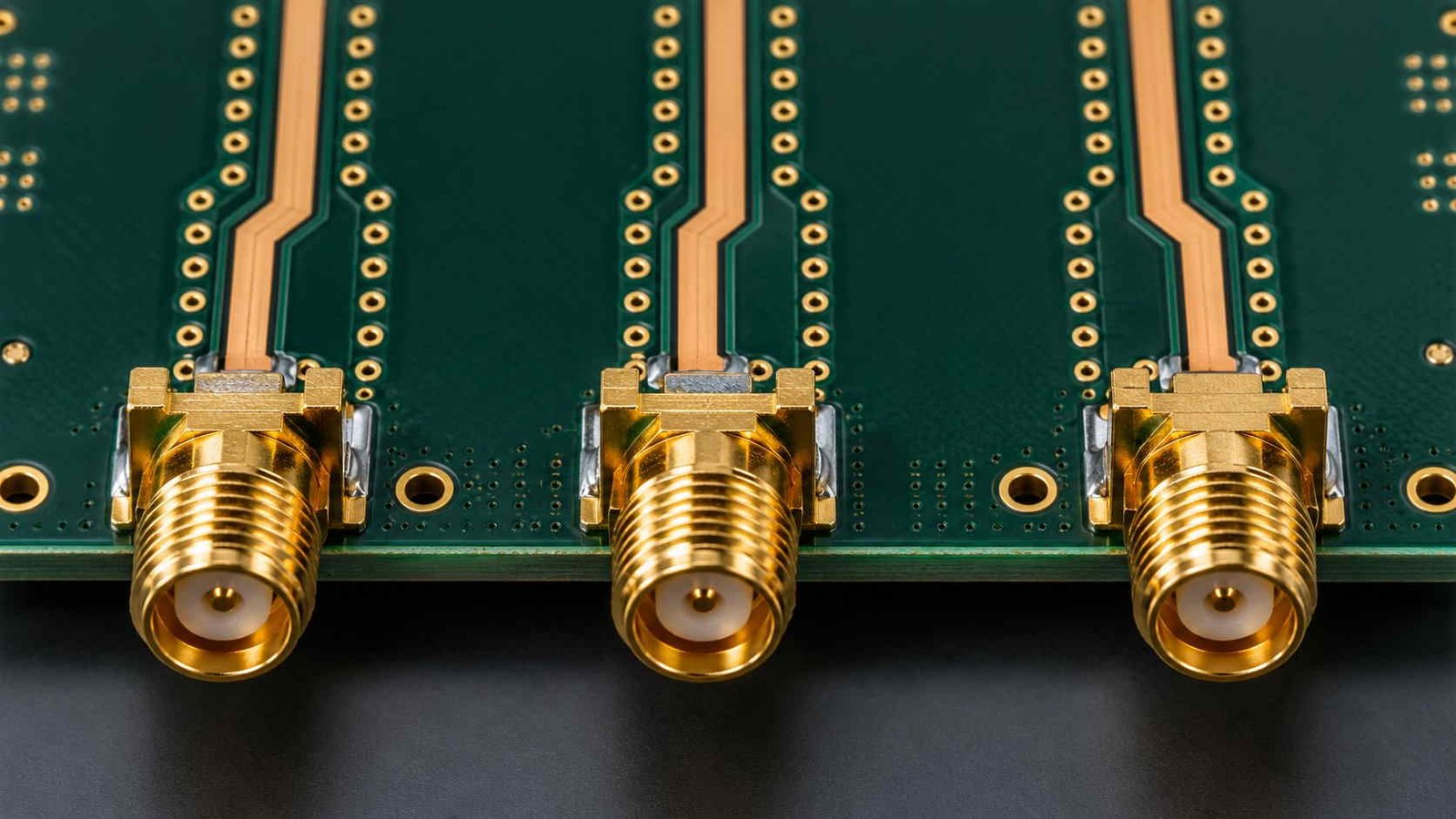
λg = λ0/√εr. Automated vector transceivers in the reported PXI class now reach 26.5 GHz, and at that frequency the fixture’s own launch — pad stack, anti-pad, first return via — contributes phase at nearly 60 degrees per millimetre. A load board designed with digital-layout habits reads DUT performance plus a few tens of degrees of fixture; a fixture designed as an RF structure can be de-embedded. Launch geometry and de-embedding method are set out in our RF connector launch and RF/mmWave test fixture guides.
At 59°/mm, the pad stack, anti-pad and first return via are not details; they are the calibration reference the whole rack leans on. A load board whose launches were left as layout defaults contributes tens of degrees of unknown phase to every S-parameter it reports — and de-embedding can only remove structure that was designed to be modelled. The launch and de-embedding method are set out in our RF connector launch guide; the probe-side treatment in the test fixture guide.
3. Fixture Loss Is a Measurement Error — Unless It Is Known
The cascade arithmetic for a passive path ahead of the DUT is unforgiving, and the table prices it.
| Uncorrected fixture insertion loss | DUT gain reads | DUT noise figure reads | Practical consequence |
|---|---|---|---|
| 0.5 dB | −0.5 dB | +0.5 dB | Small — but it never stays 0.5 dB as the fixture wears |
| 1.0 dB | −1.0 dB | +1.0 dB | Margin-eating on pass/fail lines set tight |
| 2.0 dB | −2.0 dB | +2.0 dB | A 2 dB NF shift fails good DUTs and passes bad ones |
| 4.0 dB | −4.0 dB | +4.0 dB | The test now measures the fixture, not the device |
Cascade arithmetic for a passive lossy path ahead of the DUT: uncorrected, the fixture loss adds directly to the measured noise figure and subtracts from measured gain. The remedy is not a lower-loss board — some loss is physics — but a known and stable loss: fixture-aware calibration (de-embedding the launch and path from coupon data) folds the fixture out of the result. What calibration cannot absorb is drift between calibration and test, which is why the next two tables matter: one term you might blame on temperature turns out to be minor, and the term that actually moves results is mechanical wear.
Read the 2 dB row against a real production line: a fixture that adds 2 dB of uncorrected loss fails marginally-good amplifiers and passes marginally-bad ones, and the pass/fail line everyone trusts is measuring the board. The remedy is not chasing zero loss — some is physics — but making the loss known, modelled and stable: a coupon-based de-embedding model, a written loss budget, and a service interval that re-measures the path as the fixture ages. That last word is the subject of section 5.
4. Parallel Test: Channel Phase Is Part of the Spec
Parallel test is the economic argument for automated racks — and it multiplies every fixture mismatch across every site. The table converts length spread into phase.
| Channel length mismatch ΔL | @ 12 GHz | @ 18 GHz | @ 26.5 GHz |
|---|---|---|---|
| ±0.10 mm (coupon-verified matching) | ±2.7° | ±4.0° | ±5.9° |
| ±0.25 mm (normal production spread) | ±6.7° | ±10.1° | ±14.8° |
| ±0.50 mm (digital-layout habits) | ±13.4° | ±20.2° | ±29.7° |
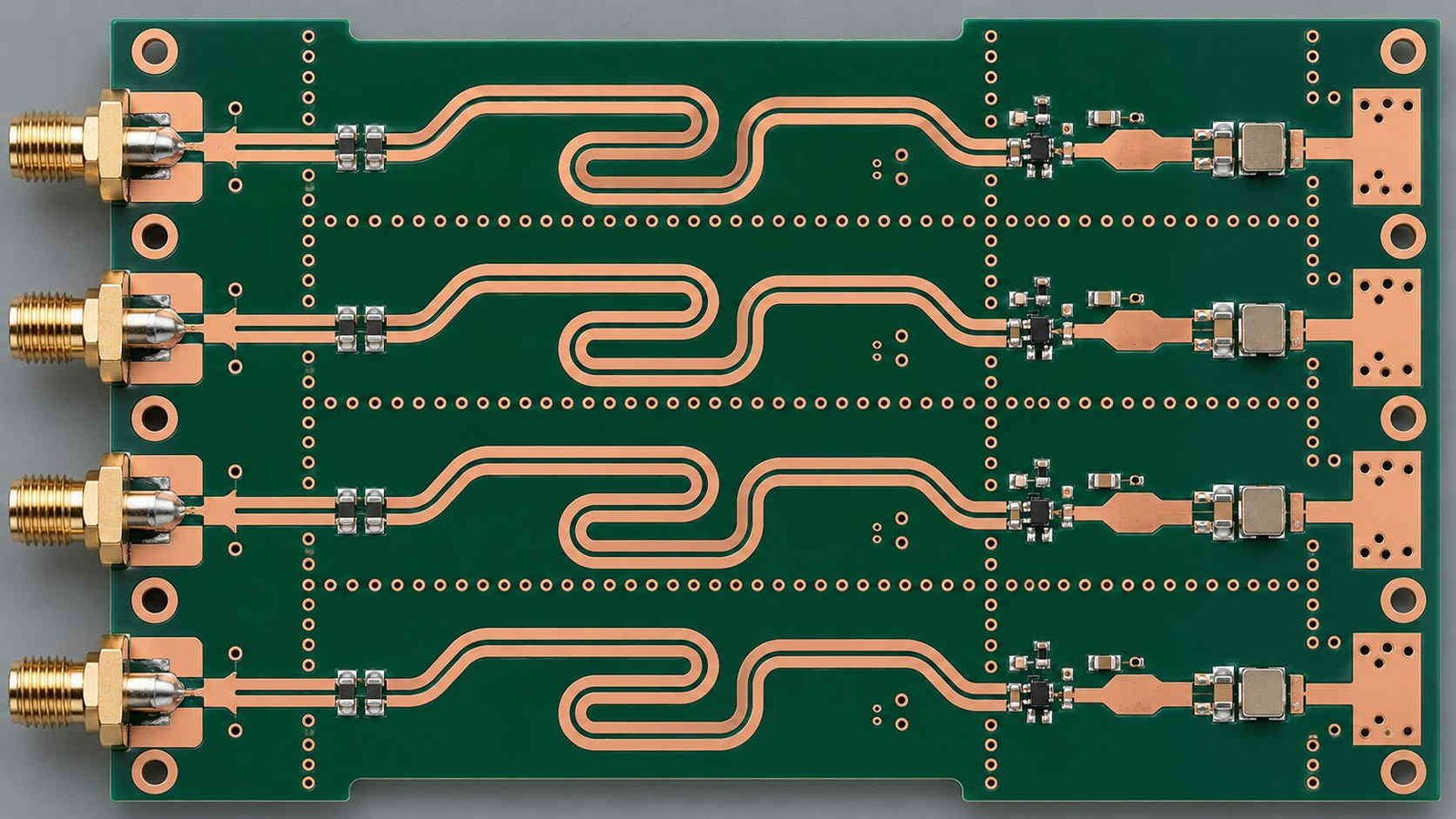
phase = 360·L·√εr·f/c. Multi-DUT parallel test — the entire economic argument for automated PXI racks — multiplies every channel mismatch across every test site: a phase-spec measurement that passes on site 1 can fail on site 4 purely from fixture spread. Length matching at ±0.10 mm, verified on the coupon, is what makes parallel sites interchangeable; at ±0.5 mm the fixtures cannot share a test limit. For scale, the temperature term people suspect first is small: a 50 mm path drifting 10 °C on a ~30 ppm/°C-class laminate moves under 1° even at 26.5 GHz (stated assumption) — mechanical geometry, not thermal, is the term to engineer.
The verdict: coupon-verified ±0.10 mm matching keeps sites interchangeable; digital-layout tolerances make the same DUT fail on one site and pass on another. And note the honest footnote — the thermal term people suspect first is minor (under 1° for a 10 °C swing on a 50 mm path, stated assumption), which is exactly why the effort belongs on geometry: it is the term that actually moves, and the term you can control on the drawing. Matching and coupon discipline follow the same method as our controlled impedance RF PCB builds.
5. The Fixture Is a Consumable: Cycles, Rework and Re-Verification
Every mate wears the contact slightly; the rating arrives sooner than intuition suggests. The table converts cycle ratings into calendar time.
| Rated mating cycles (stated assumption class) | 25 mates/day | 50 mates/day | 100 mates/day |
|---|---|---|---|
| 5,000 cycles | 200 days ≈ 6.7 months | 100 days ≈ 3.3 months | 50 days ≈ 1.7 months |
| 10,000 cycles | 400 days ≈ 13 months | 200 days ≈ 6.7 months | 100 days ≈ 3.3 months |
Cycle figures are stated assumption classes typical of high-density rack connectors — confirm against the connector datasheet for the actual part. The table turns an abstract rating into a maintenance schedule: a production fixture mated fifty times a day reaches its rated life in a few months, and contact resistance grows across that span. Two consequences for the board: coupons and launch dimensions must be re-verifiable after rework or connector replacement, and the loss/phase budget needs a service interval — a fixture whose insertion loss is re-measured monthly drifts far less than one trusted from its first-day calibration. Production-test discipline for the boards themselves is treated in our quality control and inspection overview.
A fixture mated fifty times a day spends its 10,000-cycle rating in about seven months — inside the life of the product programme it was built for. So the drawing must answer maintenance questions at design time: connector lands that support replacement, coupons and launch dimensions that stay measurable after rework, and a loss budget tied to a service interval. Fixtures designed for re-verification keep their de-embedding model honest; fixtures designed as one-shot boards quietly retire the model and the accuracy with it. The inspection side is treated in our quality control and inspection overview.
6. The DFM Checklist Before the Fixture RFQ
Nothing here is exotic; each line traces to a number computed above.
| # | Drawing or PO line item | Why it is on the list |
|---|---|---|
| 1 | Launch geometry on the drawing: pad, anti-pad, first return via — with tolerances | 59.4°/mm at 26.5 GHz (section 2) |
| 2 | Fixture-aware de-embedding: coupon-based path model, not just end-to-end cal | Loss reads as DUT error when uncorrected (section 3) |
| 3 | Loss budget written down: target insertion loss and allowed drift per service interval | Section 3 + connector wear (section 5) |
| 4 | Parallel-site channels length-matched ±0.10 mm, coupon-verified | ±5.9°/0.1 mm at 26.5 GHz (section 4) |
| 5 | Reference/sync routing kept clear of RF paths on the fixture | Repeatability depends on reference integrity (section 1) |
| 6 | Connector lands specified for rework: cycle rating and replacement procedure | Life is months, not years (section 5) |
| 7 | Backdrill residual stub ≤ 1.0 mm on RF paths in thick fixture boards | Stub resonances detune the de-embedded model |
| 8 | IPC Class 3 evidence package: microsection, coupon S-parameters per lot | Auditable repeatability, lot after lot |
Eight lines, each tracing to a number computed above. Items 1–3 make the fixture’s contribution known and removable; 4 makes parallel sites interchangeable; 5–8 make the fixture maintainable and auditable across its service life. A load board that ships with these eight answered turns the automated rack from a source of drift into a source of data.
The pattern: a PXI load board is bought as hardware but delivered as a measurement standard. For the adjacent decisions — laminate choice for the RF path, receiver-side boards that these racks characterise, or the radar modules that share the bench — the PCB material comparison chart, the direct sampling receiver PCB guide, the X/Ku-band AESA radar PCB guide and our RF PCB manufacturer overview are the right starting points. The wideband measurement context behind many test plans is in the EW PCB wideband design guide.
PXI RF Test Fixture PCB — Frequently Asked Questions
What a load board is, why calibration alone is not enough, parallel-site phase matching, mating-cycle maintenance, and what the RFQ should contain.
What is a PXI RF test fixture / load board?
It is the interface board that carries the device under test in an automated PXI rack: PXI RF instruments on one side, the DUT socket or launch on the other, and whatever switching, attenuation and coupling the test plan needs in between. In reported EuMW 2026 demonstrations, modular PXI platforms with vector signal transceivers and FPGA automation ran S-parameter, compression, intermodulation, noise-figure and pulse measurements — every one of them quoted through this board. The fixture is not wiring; it is part of the measurement chain.
If the VNA can calibrate the fixture out, why does fixture loss matter?
Because calibration removes what is known and stable at calibration time. A 2 dB fixture path reads as −2 dB of DUT gain and +2 dB of noise figure when uncorrected — and it does not stay 2 dB: connector wear, contact resistance growth and rework all move the path between calibrations. The practical standard is a fixture-aware de-embedding model built from coupon measurements, plus a written loss budget and a service interval, so what changes between calibrations is measured, not hoped away.
How closely must parallel test channels be matched?
Tight enough that test sites are interchangeable: length matching at ±0.10 mm, verified on coupons, holds channel phase within about ±6° even at 26.5 GHz. At ±0.5 mm of production spread the same measurement differs by nearly 30° between sites at 26.5 GHz — enough to fail a phase-spec DUT on one site and pass it on another. Notably, temperature is the smaller term: a 50 mm path over a 10 °C swing drifts under 1° on a typical laminate, so geometry and wear deserve the engineering effort, not thermal compensation.
Is the fixture a one-time purchase?
No — it is a consumable with a maintenance schedule. High-density rack connectors carry cycle ratings in the thousands; a production fixture mated 50 times a day reaches a 10,000-cycle rating in about seven months, with contact resistance growing across that span. Specify connector lands for rework, keep coupons and launch dimensions re-verifiable after replacement, and re-measure insertion loss on a service interval. A load board designed for re-verification outlives several generations of DUT sockets.
What should a PXI fixture RFQ include?
The facts that size the board: DUT interface type and pin-out, frequency range and the measurement types planned (S-parameters, NF, intermod, pulse), number of parallel test sites, mating-cycle estimate per day, and the acceptance evidence expected — coupon S-parameters, launch de-embedding data, length-matching verification, IPC Class 3 microsections. Suppliers who ask for the measurement plan before quoting are designing the fixture as an RF structure, not quoting a blank.
Building PXI load boards or RF test fixtures?
Send us the DUT interface, frequency range, measurement plan and parallel-site count. We will review the launch geometry, loss budget, channel matching and connector-rework plan at stackup review, and quote the fixture with coupon S-parameters, de-embedding data and IPC Class 3 evidence.
Contact Us → WhatsApp: +86 137 6047 3650Request a PCB Quote
Upload your Gerber ZIP file and project requirements. Our engineering team will review your PCB material, stackup, impedance needs, surface finish, and production quantity before quoting.
Please prepare:
- Gerber files in ZIP format
- PCB material or stackup requirements
- Controlled impedance notes if available
- Prototype or batch production quantity