Controlled Impedance PCB Manufacturer — ±5% TDR Every Lot

Riching PCB manufactures controlled impedance PCB on Rogers RO4350B, RO3003, RT5880 and FR4. ±10% standard, ±5% available with TDR measurement and report on every production lot. Min trace/space 2.5mil for tight RF routing. In-house plasma activation for PTFE materials. 7–10 day prototype. No MOQ.

Table of Contents

±5%

TDR available
report per panel

2.5mil

min trace/space
advanced routing

In stock

RO4350B · RO3003
RT5880

7–10

day prototype
no MOQ

Impedance Tolerance Options

ToleranceVerificationTypical ApplicationLead Time Impact
±10% (standard)Sample-based TDRGeneral RF, EW, satcomNo impact
±5% (tight)TDR every panel + reportPhased array, 77GHz radar+1–2 days
±5% + single-lot materialTDR per panel + lot certificateMulti-panel phased array, AESAConfirm on enquiry

±10% impedance tolerance is standard for most RF and digital high-speed designs and is verified via sample-based TDR measurement. For applications where amplitude or phase consistency across an array matters — phased array PCB, 77GHz radar PCB, or Ka-band PCB — ±5% tolerance with TDR measurement and report on every panel is available. Specify on the stackup drawing.

What Affects Impedance — and How We Control It

FactorAffects Impedance ByRiching PCB Control
Dielectric thicknessDirect — thicker = higher Z0 (microstrip)Production Dk certificate per lot
Trace widthDirect — narrower = higher Z0Etch compensation per copper weight
Copper weightIndirect — thicker copper widens effective traceEtch factor calibrated 0.5oz–2oz
Dielectric constant (Dk)Direct — higher Dk = lower Z0Material lot Dk verified vs datasheet
Soldermask over traceAdds ~2–5Ω depending on thicknessLSOG thickness controlled, factored in
Reference plane distanceDirect — stripline depends on both planesStackup drawing confirms plane symmetry

Impedance is determined by trace geometry, dielectric properties and stackup — not just trace width. For the full calculation methodology and reference trace widths by material and copper weight, see 50Ω RF trace PCB design guide.

TDR Verification ProcessTDR impedance verification process diagram showing measurement points on PCB panel for controlled impedance manufacturing

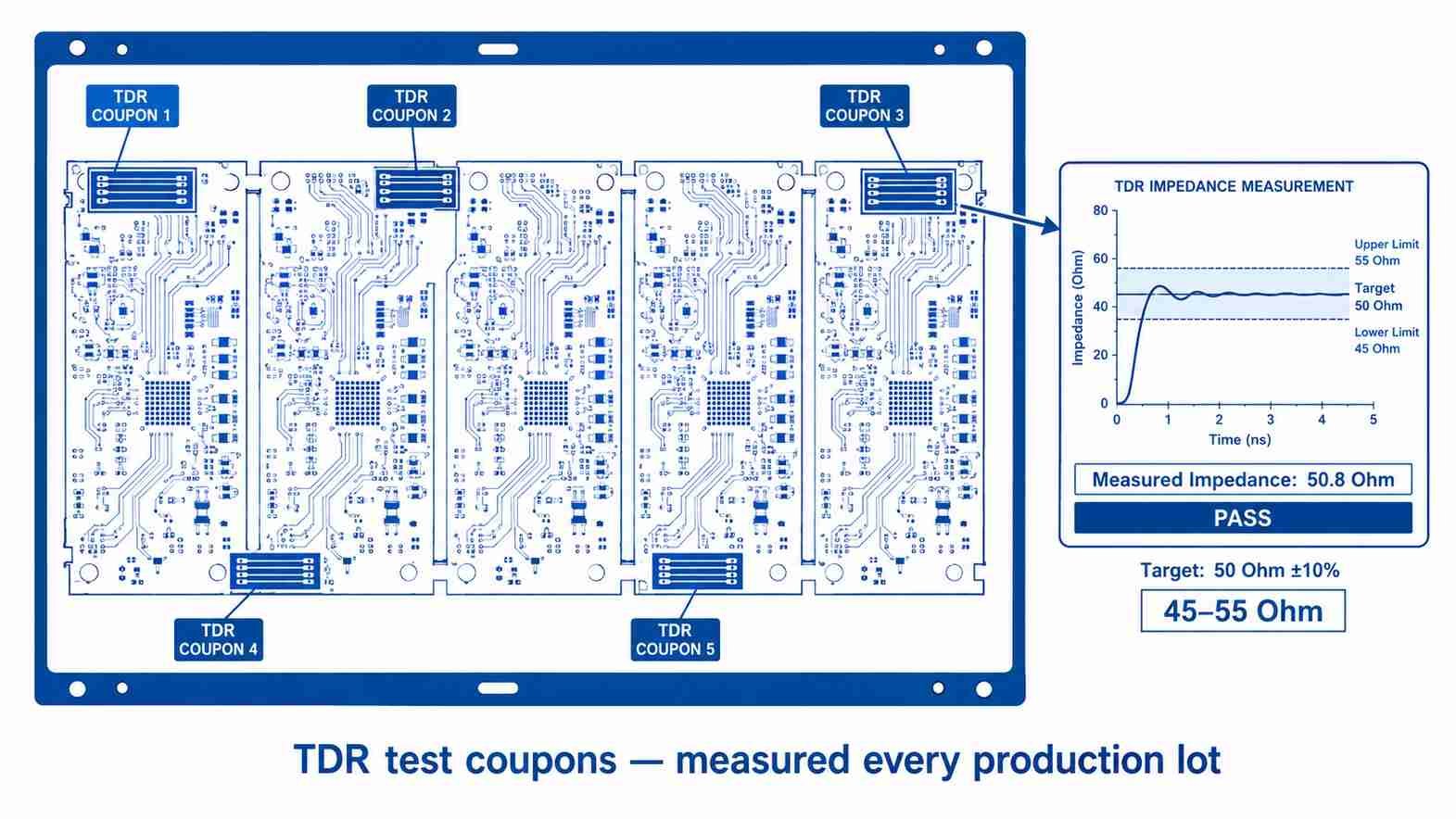
  • TDR test coupons placed on every production panel — not just first-article
  • Measurement performed before shipment — out-of-spec panels are identified and addressed before delivery
  • TDR report available on request — includes measured impedance per coupon location
  • For PTFE materials, TDR follows the in-house plasma activationand lamination steps — see PTFE PCB manufacturer for the full process.

Materials Supporting Controlled Impedance

  • Rogers RO4350B / RO4003C— in stock, ±10% standard, FR4-compatible process
  • Rogers RO3003— in stock 0.127 / 0.254mm, ±5% available for Ka-band and 77GHz
  • Rogers RT5880— in stock 6 thicknesses, lowest Df for wideband impedance stability
  • FR4 — standard ±10%, digital high-speed and mixed-signal designs

Process Capabilities

  • Min trace/space 3mil/3mil standard, 2.5mil/2.5mil advanced — tighter routing for impedance-critical designs
  • Production Dk certificate provided per material lot
  • Etch compensation calibrated per copper weight (0.5oz–2oz)
  • Stackup drawing confirms symmetric/asymmetric stripline reference plane distances
  • IPC Class 2 standard, Class 3 on request

How to Order

  • WhatsApp: +86 13760473650
  • Send: Gerber zip + NC drill + stackup drawing
  • Specify: target impedance (e.g. 50Ω), tolerance (±10% or ±5%), reference layer/plane
  • DFM review confirms trace width vs production Dk before fabrication: 4–8 hours
  • No MOQ. From 1 board.

Controlled Impedance PCB Manufacturer — Shenzhen Direct Factory

±5% TDR Every Lot · RO4350B RO3003 RT5880 In Stock
2.5mil Min Trace · 7–10 Day Prototype · No MOQ

Send Gerber + stackup drawing. DFM review within 4–8 hours.
Specify target impedance, tolerance and reference layer.

WhatsApp +86 13760473650

DFM review within 4–8 hours

PCB Project Review

Request a PCB Quote

Upload your Gerber ZIP file and project requirements. Our engineering team will review your PCB material, stackup, impedance needs, surface finish, and production quantity before quoting.

Please prepare:

  • Gerber files in ZIP format
  • PCB material or stackup requirements
  • Controlled impedance notes if available
  • Prototype or batch production quantity
ZIP format only. Please compress all Gerber and drill files into one ZIP package before uploading.