High Frequency PCB DFM Review — Free, 4–8 Hour Turnaround
Every order goes through a free DFM (Design for Manufacturability) review before fabrication — typically returned within 4–8 hours alongside your quote. For Rogers, PTFE, Taconic and F4B designs, this catches the issues that cause field failures: impedance mismatches, insufficient via fence isolation, excess lamination cycles and stackup errors.
Home » DFM review PCB » High Frequency PCB DFM Review — Free, 4–8 Hour Turnaround
Table of Contents
Free
DFM review
with every quote
4–8 hrs
turnaround
returned with quote
9-point
checklist
impedance to stackup
No MOQ
From 1 board
Rogers · PTFE · FR4
Why DFM Review Matters for High Frequency PCB
High frequency PCB issues often pass initial visual inspection and electrical continuity testing — and fail only after thermal cycling or in RF performance testing. By the time a board fails in the field, the cost of rework is far higher than catching the issue at the design stage. See PTFE PCB manufacturing: 5 mistakes that cause field failures for examples of issues that DFM review is designed to catch.
What We Check in a DFM Review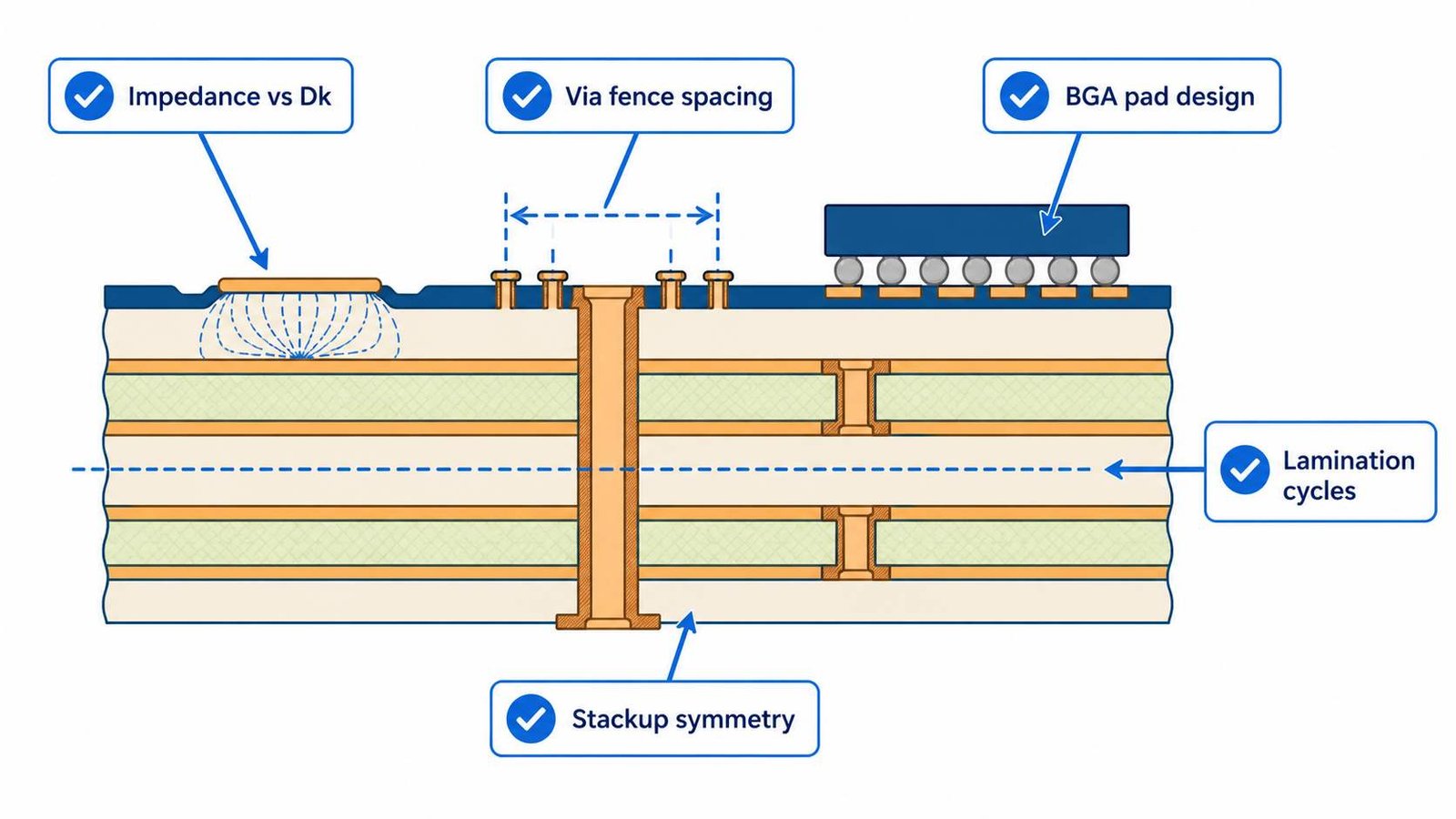
| Check Item | What We Verify | Catches |
|---|---|---|
| Impedance vs production Dk | Trace width against actual material lot Dk certificate | Impedance out of spec at delivery |
| Via fence spacing vs frequency | Center-to-center spacing against λ/10 at operating frequency | Insufficient isolation, signal leakage |
| Lamination cycle count (PTFE) | Number of press cycles required by stackup | Dk shift, delamination risk |
| BGA / fine-pitch pad design | Annular ring vs min drill capability | Pad lift, plating voids |
| Plating hole design (resin/copper plug) | Hole design vs lamination cycle and copper thickness rules | Blind/buried via reliability issues |
| Panel utilization | Board layout vs standard panel sizes | Unnecessary cost from poor utilization |
| Surface finish vs application | ENIG / hard gold / ENEPIG suitability for design | Wrong finish for application (e.g. wire bonding) |
| Stackup symmetry | Reference plane distances for stripline designs | Impedance calculation errors |
Impedance Verification
For controlled impedance designs, DFM review confirms trace width against the production material’s actual Dk certificate — not just the datasheet nominal value. See controlled impedance PCB manufacturer for tolerance options, and why RF PCB fails impedance testing for common root causes.
Via Fence and Isolation
For antenna arrays, filters and shielded RF sections, via fence spacing is checked against λ/10 at the operating frequency. See RF via fence PCB for design rules — this is especially critical for 77GHz radar and phased array designs where via fence pitch must scale with frequency.
PTFE-Specific Checks
- Lamination cycle count — max 2 cycles enforced, see PTFE PCB manufacturer
- Drill parameters — PTFE-specific 40-60K RPM vs FR4 speed, see PTFE PCB plasma activation
- Plasma activation window compatibility with stackup design
- Material lot Dk verification against design assumptions
How DFM Review Fits the Order Process
- Send Gerber + drill + stackup drawing via WhatsApp
- DFM review + quote returned together: 4–8 hours
- Any issues found are flagged with suggested corrections before fabrication starts
- Once approved, fabrication begins — see high frequency PCB prototype manufacturerfor lead times by material
How to Submit for DFM Review
- WhatsApp: +86 13760473650
- Send: Gerber zip + NC drill + stackup drawing
- Specify: impedance target/tolerance, IPC Class, any special process notes
- Review + quote: 4–8 hours
- No MOQ. From 1 board.
High Frequency PCB DFM Review — Shenzhen Direct Factory
Free DFM Review in 4–8 Hours
Rogers · PTFE · FR4 · No MOQ
Send Gerber + drill + stackup drawing.
Quote and DFM feedback returned together.
Quote + DFM feedback together
Request a PCB Quote
Upload your Gerber ZIP file and project requirements. Our engineering team will review your PCB material, stackup, impedance needs, surface finish, and production quantity before quoting.
Please prepare:
- Gerber files in ZIP format
- PCB material or stackup requirements
- Controlled impedance notes if available
- Prototype or batch production quantity