
Ku-Band BUC PCB: Designing the Board Group Behind a 200–400 W Satellite Uplink
Ku-band BUC and SSPA PCB guide: GaN thermal design for 200-400 W uplink amplifiers, 50 V bias IR drop, WR75 transitions, monitor and redundancy boards.
Table of Contents
Every satellite earth station uplink ends in the same place: a block-upconverter that takes the L-band IF, lifts it to the 13.75–14.5 GHz Ku uplink band, and amplifies it to hundreds of watts into the feed. The product class is refreshed regularly — the newly published Ku-band GaN BUC/SSPA data adds 200 W and 400 W rated units with 100 W and 200 W linear power, integrated monitoring and redundancy support — and each of those units is, from the fabricator’s side, a board group with very specific arithmetic attached.
This page computes that arithmetic: why the board group, not the RF board, is the product; why the thermal budget follows dissipated watts rather than rated output; why a thermal via array is off by three orders of magnitude at this power; what a 50 V rail at 23 amperes does to an undersized bias trace; what 14 GHz looks like on the RF board; and why the WR75 transition is a broadband structure with tolerances on the drawing. Every figure is computed; the assumptions are stated where they are used.
The satellite materials side — laminate choice for space and ground segments — is treated in our satellite communication PCB overview, and the general PA stackup logic in the RF power amplifier PCB design guide. This page is about the uplink amplifier itself: the board group behind a 200–400 W Ku-band BUC.
1. What a BUC Is — and Why You Are Buying a Board Group
A BUC is sold as one sealed unit, but it is engineered as a stack of boards with different disciplines. The table maps the group.
| Board in the BUC group | What it carries | What the fabricator must confirm |
|---|---|---|
| RF amplifier chain board | 14 GHz gain stages, 13.75–14.5 GHz output network, bias injection | Low-loss laminate, heavy copper, phase-controlled output combining |
| Control & monitor board | RS-232/RS-485 and Ethernet telemetry, alarms, LNB bias and data logging | Isolation between monitor lines and RF sections; connector mapping |
| Power distribution board | 50 V drain rail at 20+ amperes, sequencing, fault interlocks | Rail copper weight and IR drop sized to the current, not assumed |
| Redundancy & switching board | 1:1 / 1:2 changeover, waveguide or coax switch control | Status feedback lines, fail-safe behaviour on power loss |
| Test fixture & coupons | Launch de-embedding, loss-trend and phase coupons for the RF board | Coupon set agreed before production, not after first article |
A block-upconverter is sold as one unit, but it arrives as a board group: the RF chain, the control and monitoring layer (the reported Ku-band GaN BUC product class integrates RS-232/485 and Ethernet monitoring, LNB bias and data logging), the power distribution layer, and the redundancy switching that uplink operators require. Quoting only the RF board misprices the product — the control and power boards decide whether the amplifier survives in the field, and the coupon set decides whether its performance can be verified lot by lot.
Two rows decide most field failures. The power distribution board carries a rail that hundreds of watts depend on — and its copper weight is a stackup decision, not a layout afterthought. The control and monitor board carries the telemetry and bias functions that operators configure over RS-485 or Ethernet, and its isolation from the RF sections decides whether the unit is serviceable in a rack. A supplier who quotes the RF chain and prices the rest as “simple” has not read the product; the reported Ku-band GaN BUC class integrates monitoring, LNB bias, data logging and redundancy configuration precisely because these functions are the product.
2. Rated vs Linear Power: the Number That Sets the Thermal Budget
BUC datasheets quote two output powers, and buyers often quote thermal design from the wrong one. The table separates them.
| Operating point (reported 200/400 W-class Ku GaN BUC) | RF output | What it implies |
|---|---|---|
| Rated (saturated) power | 200 W / 400 W | The headline number — and the highest-efficiency point |
| Linear power | 100 W / 200 W | 3 dB back-off; the honest number for multi-carrier uplinks |
| −6 dB OBO (multi-carrier) | 50 W / 100 W | Extra back-off per carrier loading; linearity, not power, is now the limit |
| Heat dissipated at rated output (η = 35% assumed) | 371 W / 743 W | The number the thermal design must be quoted against — not the RF output |
P_heat = P_dc − P_rf with P_dc = P_rf/η; η = 35% is a stated calculation assumption for a Ku GaN power stage, not a device datasheet value. The asymmetry is the point: a "400 W" amplifier dissipates roughly 743 W at rated output before any back-off, and back-off for multi-carrier linearity does not reduce the rail voltage — it changes where on the load line the device sits. Thermal design, baseplate interface and cooling specification follow the dissipated watts; the material and stackup review follows the RF output. The general PA material logic is treated in our RF power amplifier PCB review and the PA design guide.
The last row is the quote-defining number: at a stated 35% efficiency assumption, the 400 W-class unit dissipates about 743 W at rated output — and that is before multi-carrier back-off moves the operating point for linearity. Two consequences follow. First, thermal design, baseplate interface and cooling specification are quoted against dissipated watts, which is why a serious fabricator asks for rated power, linear power and duty cycle before proposing a stackup. Second, the RF material choice follows the frequency and output network, not the power rating alone — the material review logic is the same as any power amplifier, in our RF power amplifier PCB review.
3. The Thermal Path: the Baseplate Carries It, Not the Via Array
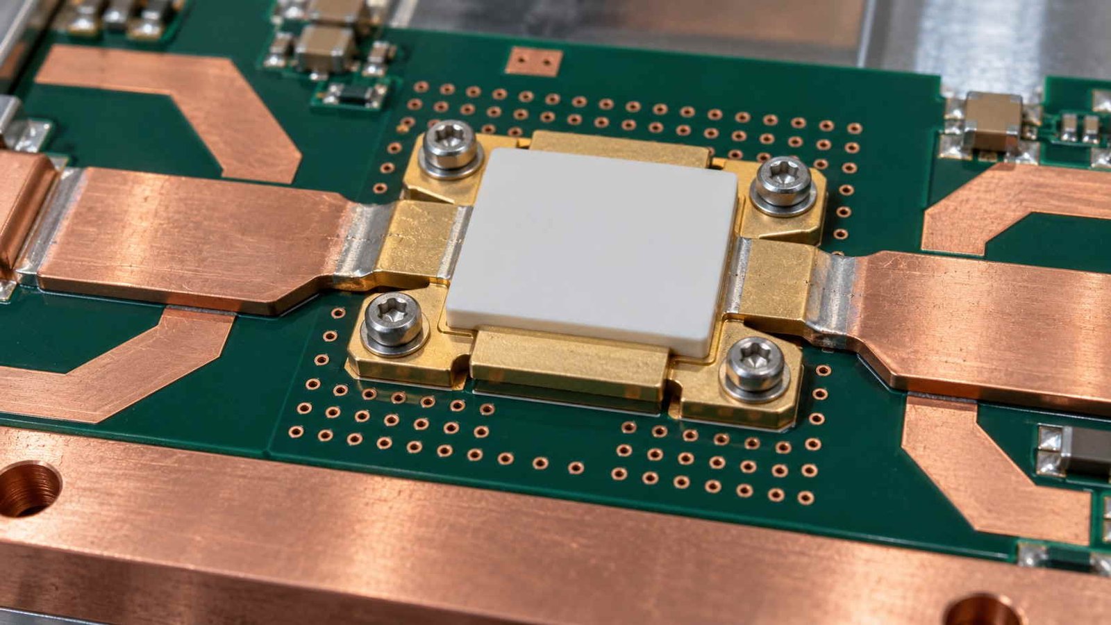
At 10 W, thermal vias are the standard answer. At 371 W, the same answer is off by three orders of magnitude — and the table shows why.
| Thermal element (371 W heat, one 200 W-linear module) | Thermal resistance | ΔT across the element |
|---|---|---|
| Copper spreader 2 mm (r 15→60 mm) | 0.283 K/W | 105 K — already marginal |
| Copper spreader 3 mm | 0.189 K/W | 70 K |
| Copper spreader 5 mm | 0.113 K/W | 42 K — workable with forced cooling |
| 36-via thermal array alone (0.8 mm, L = 3 mm) | 3.40 K/W | 1,262 K — physically impossible; vias are not the baseplate |
Spreading R = ln(r2/r1)/(2π·k·t), k = 390 W/mK; via-array R = (L/(k·A_wall))/36 in parallel. The verdict row is the design driver: at hundreds of watts, board-level thermal via arrays — the right answer for a 10 W device — are off by three orders of magnitude. Flanged GaN power transistors in this class mount through the PCB onto a metal carrier or baseplate, and the baseplate thickness, flatness under the flange and the joint to the heatsink are thermal specifications that belong in the fabrication drawing set. The via array still matters — for the LNA and control sections, and to tie ground planes around the RF chain. Device-level thermal via and ground-pad design for GaN is treated in our GaN RF power amplifier thermal guide; the chassis and environment side in the massive MIMO thermal guide.
The verdict row is not an exaggeration for effect: 36 parallel vias of 0.8 mm diameter and 3 mm length present about 3.4 K/W, and 371 W across that is a temperature no material survives. Flanged GaN power transistors at this class mount through the PCB onto a metal carrier or baseplate — so the PCB fabricator’s deliverables are different from a typical RF board: the baseplate or carrier specification, the flange-flatness mounting zone, the counterbore or cutout tolerances, and the joint to the heatsink. The via array keeps its job where it belongs: the LNA and control sections, and stitching ground around the RF chain. Device-level thermal design is treated in our GaN RF power amplifier thermal guide.
4. The 50 V Bias Rail: IR Drop at 23 Amperes
GaN moves the efficiency story forward, but the drain rail still moves serious current. The table sizes it.
| 50 V drain rail (L = 100 mm) | Resistance | @ 23 A (400 W RF, η = 35%) | Rail loss |
|---|---|---|---|
| 1 oz, 5 mm wide | 9.85 mΩ | 0.227 V | 5.2 W of extra heating |
| 2 oz, 10 mm wide | 2.46 mΩ | 0.057 V | 1.3 W |
| 3 oz, 15 mm wide | 1.09 mΩ | 0.025 V | 0.6 W |
R = ρ·L/(w·t) at 20 °C, hot copper is worse; 400 W RF at 50 V and 35% efficiency draws about 23 A, and the current scales with every efficiency point the PA loses. A 1 oz / 5 mm rail converts that into a quarter-volt of sag and 5 W of rail self-heating on top of the 743 W the PA stage is already dumping — on the board that has to stay flat enough for the flange joint. Rail copper weight, width and route length are stackup-review decisions, and the decoupling and sequencing around the rail belong on the power distribution board, not in a copper-pour afterthought.
Two things make this row worth a drawing line. The voltage sag is small in isolation but sits directly on the drain bias that sets the PA’s operating point — a quarter volt of IR drop is a design variable, not noise. And the rail self-heating lands on the same board that must stay flat enough for the flange-to-baseplate joint, which is why rail copper weight, width and route length are agreed at stackup review with the thermal budget attached. On the power distribution board, sequencing and fault interlocks protect the expensive die; on the RF board, the rail is a copper decision.
5. The 14 GHz Board: Phase per Millimetre on the RF Chain
13.75–14.5 GHz sounds comfortably below the mmWave threshold — until the wavelength arithmetic is done on the board.
| Geometry on the 14 GHz RF board (εr 3.48 class) | Value | Design consequence |
|---|---|---|
| Free-space wavelength λ0 | 21.4 mm | — |
| In-medium wavelength λg | 11.5 mm | λ/4 networks are ~2.9 mm — etch tolerance is a circuit tolerance |
| Phase per millimetre | 31.4°/mm | Output combining networks are phase devices, not traces |
| 3 mm residual via stub resonance | 13.4 GHz | At the 13.75 GHz band edge — un-backdrilled through vias are unusable on the RF chain |
λg = λ0/√εr; stub resonance f = c/(4·L·√εr). At 14 GHz one millimetre of unplanned geometry is 31 degrees, so the output combiner, bias tees and coupling structures are dimensioned to tens of microns and verified on coupons. The stub row closes the argument: a 3 mm board with un-backdrilled through vias puts a resonance at 13.4 GHz — touching the band edge — so the RF chain is backdrilled or blind/laser by design, with residual stub verified by microsection or x-ray per panel. Tolerances and method are in our back drill PCB guide and drilling capabilities page; impedance and phase discipline in the controlled impedance RF PCB and 50 ohm trace guides.
The phase row is the one that disciplines the layout: at 31.4°/mm, the output combining network and the bias tees are phase devices with tens-of-micron sensitivities, verified on coupons rather than trusted from CAD. The stub row is the manufacturing consequence: on a 3 mm board — and BUC boards are thick, because they carry the rail and the stiffness — every un-backdrilled through via on the RF chain is a 13.4 GHz resonance sitting on the band edge. Backdrill or blind/laser by design, residual stub as a specified dimension, microsection or x-ray per panel.
6. The WR75 Launch: Where Microstrip Meets Waveguide
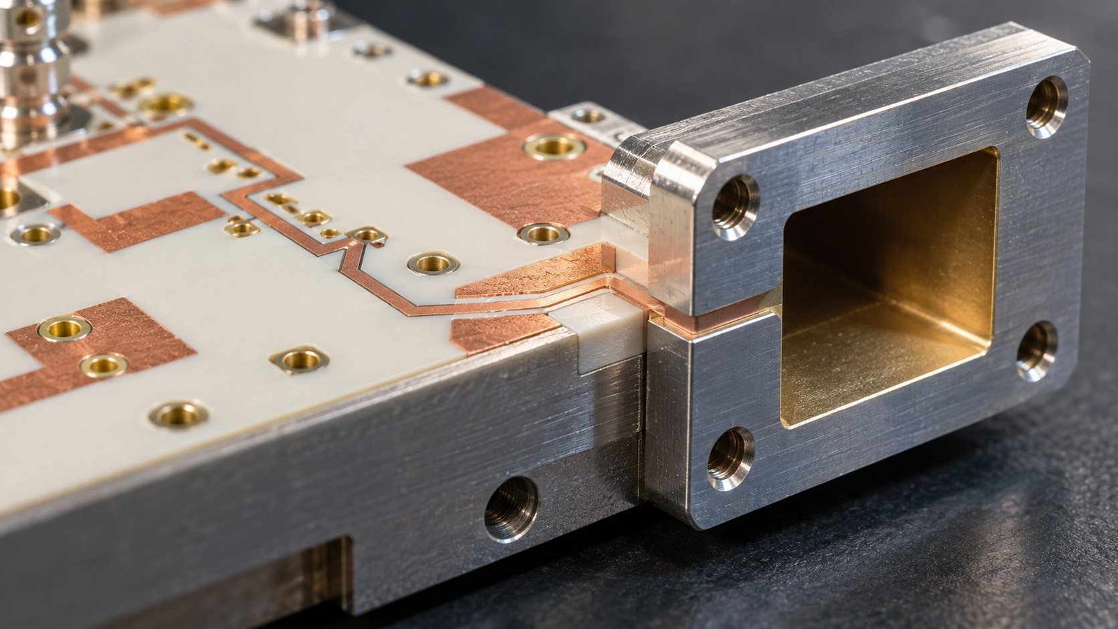
The output transition is where the amplifier meets the antenna feed, and in Ku band it is a waveguide: WR75, flange-mounted at the board edge. The table shows the broadband problem.
| Frequency (Ku uplink band) | Free-space λ0 | WR75 guide wavelength λg | Transition design implication |
|---|---|---|---|
| 13.75 GHz | 21.80 mm | 26.59 mm | Probe and back-short distances start long |
| 14.25 GHz | 21.04 mm | 25.23 mm | Mid-band reference |
| 14.50 GHz | 20.68 mm | 24.61 mm | λg runs 2 mm shorter than band edge — a narrowband transition detunes |
WR75 (a = 19.05 mm) has a TE10 cutoff of 7.87 GHz, well below the 13.75–14.5 GHz uplink band, and the guide wavelength varies about 7.5% across the band — enough to detune a transition designed at one frequency. The microstrip-to-waveguide probe, its back-short spacing and the K-slot aperture are therefore broadband structures with tolerances on the drawing, verified by de-embedded measurement rather than asserted. The design method and loss budget are set out in our PCB-to-waveguide transition guide; the measurement side in the mmWave VNA testing and test fixture guides.
A probe transition dimensioned at mid-band loses a millimetre and a half of guide wavelength by the band edges — enough to detune the match and shift the loss budget, which is why the probe, back-short spacing and aperture are broadband structures whose tolerances are on the fabrication drawing and whose performance is verified by de-embedded measurement on production launch geometry. The design method, loss budget and verification flow are set out in our PCB-to-waveguide transition guide and the test fixture guide.
7. The DFM Checklist Before the BUC RFQ
Nothing here is exotic; each line traces to a number computed above, and each is cheap on a drawing and expensive to reconstruct after a first article fails.
| # | Drawing or PO line item | Why it is on the list |
|---|---|---|
| 1 | Thermal design quoted to dissipated watts (371/743 W class), not RF output | Section 2 — the number the cooling and baseplate follow |
| 2 | Flanged GaN mounting: baseplate/carrier thickness and flange-flatness zone on the drawing | Via arrays are off by 3 orders of magnitude at this power (section 3) |
| 3 | 50 V rail: copper weight × width sized to 23 A with IR drop written down | 0.25 V / 5 W of avoidable rail loss (section 4) |
| 4 | RF chain backdrilled: residual stub ≤ 1.0 mm, microsection/x-ray per panel | 3 mm stub resonates at the 13.75 GHz band edge (section 5) |
| 5 | Output combining networks dimensioned to coupon-verified phase | 31.4°/mm at 14 GHz (section 5) |
| 6 | WR75 probe transition: broadband geometry, back-short and aperture tolerances on the drawing | λg shifts 2 mm across the band (section 6) |
| 7 | Monitor/control isolation: RS-485/Ethernet, LNB bias and telemetry routed clear of RF sections | The board group lives or dies in the field on this (section 1) |
| 8 | Coupon set agreed before production: launch de-embedding, loss-trend, phase | Lot-to-lot verification of everything above |
Eight lines, each tracing to a number computed above. Items 1–3 decide whether the amplifier survives its own dissipation; 4–6 decide whether it meets the uplink band; 7–8 decide whether the unit is operable and auditable in an earth-station rack. A BUC RFQ that carries these eight answers is quotable on engineering, not on laminate brand names.
The pattern across the whole page: a BUC is bought as an amplifier but delivered as an engineered system of boards, thermal interfaces and verification evidence. For the adjacent decisions — laminate selection for the RF chain, the terminal-side boards that receive the downlink, or the radar-class T/R boards that share the band — the PCB material comparison chart, the VSAT and LEO terminal PCB guide, the LEO satellite PCB design guide and the X/Ku-band AESA radar PCB guide are the right starting points, and our RF PCB manufacturer overview covers the fabrication capabilities behind all of them.
Ku-Band BUC PCB — Frequently Asked Questions
What a BUC is, rated vs linear vs dissipated power, why the baseplate carries the heat, the 14 GHz board, the WR75 transition, and what the RFQ should contain.
What does a BUC actually do, and what boards does it need?
A block-upconverter takes the modulated L-band IF (950–1700 MHz in the reported Ku-band GaN product class), upconverts it to the 13.75–14.5 GHz Ku uplink band, and amplifies it to hundreds of watts for the antenna feed. One product, several boards: the 14 GHz RF amplifier chain, a control and monitor board (RS-232/RS-485 and Ethernet telemetry, alarms, LNB bias, data logging), a power distribution board for the 50 V drain rail, and redundancy switching for 1:1/1:2 earth-station configurations. Quoting the RF board alone misprices the unit.
Should the thermal design be quoted from rated power or linear power?
From dissipated power, which is neither of those. Heat is DC input minus RF output; at a stated 35% efficiency assumption, a 200 W-linear module dissipates about 371 W and a 400 W-class unit about 743 W at rated output. Rated power is the highest-efficiency point, and multi-carrier back-off changes the operating point rather than the rail — so the baseplate, cooling and flange interface are specified against the dissipated watts, while the RF stackup follows the output frequency and power.
Can thermal vias replace a metal baseplate at 200–400 W?
No, and the arithmetic is blunt: a 36-via array of 0.8 mm, 3 mm-long plated vias presents about 3.4 K/W in parallel — over 1,200 K across 371 W. Via arrays are the right tool for 10 W-class devices and for tying ground planes; at BUC power levels the flanged GaN transistor mounts through the PCB onto a metal carrier or baseplate whose thickness, flatness under the flange, and heatsink joint are specified thermal dimensions in the drawing set.
Why is the WR75 transition a fabrication-level conversation?
Because the guide wavelength in WR75 shifts about 2 mm — roughly 7.5% — between 13.75 and 14.5 GHz, enough to detune a transition designed at a single frequency. The microstrip-to-waveguide probe, back-short spacing and aperture are broadband structures whose dimensions belong on the fabrication drawing, and their performance is verified with de-embedded measurements on the production launch geometry, not inferred from a datasheet curve.
What should a Ku-band BUC RFQ include?
The conditions that change the board: rated and linear power and the duty cycle between them, baseplate temperature class and cooling method, the flange interface of the chosen transistors, monitor and redundancy interfaces (RS-485, Ethernet, switch control), and the acceptance evidence you expect — launch de-embedding, loss-trend and phase coupons, microsection proof of backdrill depth, to IPC Class 3. Suppliers who ask for these before quoting are pricing engineering, not guessing.
Building a Ku-band BUC or SSPA board group?
Send us the rated and linear power, baseplate temperature class, transistor flange interface and monitor/redundancy interfaces. We will review the thermal path, the 50 V rail, the backdrill plan and the WR75 transition at stackup review, and quote the RF, control and power boards with launch de-embedding, loss-trend and phase coupons to IPC Class 3.
Contact Us → WhatsApp: +86 137 6047 3650Request a PCB Quote
Upload your Gerber ZIP file and project requirements. Our engineering team will review your PCB material, stackup, impedance needs, surface finish, and production quantity before quoting.
Please prepare:
- Gerber files in ZIP format
- PCB material or stackup requirements
- Controlled impedance notes if available
- Prototype or batch production quantity